

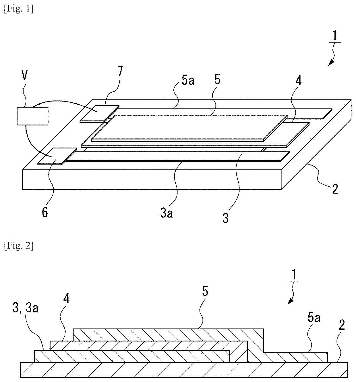
Heat flow switching element
a switching element and heat flow technology, applied in the manufacture/treatment of thermoelectric devices, lighting and heating apparatus, machine operation modes, etc., can solve the problems of plastic deformation due to mechanical contact pressure, inability to achieve reproducibility, and difficulty in size design, so as to ensure the flatness and mechanical strength of the entire element, the effect of increasing the variation of thermal conductivity and high thermal responsiveness
- Summary
- Abstract
- Description
- Claims
- Application Information
AI Technical Summary
Benefits of technology
Problems solved by technology
Method used
Image

Examples
example 1
[0085]Using the following materials, an N-type semiconductor layer, an insulator layer, a P-type semiconductor layer, and a P-side electrode were laminated on a substrate to obtain Example 1 of the present invention, and a change in thermal conductivity thereof was measured.
[0086]Substrate: glass substrate (0.5 mm thick) N-type semiconductor layer: Si0.36Ge0.56P0.08 (40 nm thick)
[0087]Insulator layer: SiO2 (30 nm thick)
[0088]P-type semiconductor layer: Si0.375Ge0.575Au0.05 (20 nm thick)
[0089]P-side electrode: Mo (100 nm thick)
[0090]Also, it was confirmed that each of Si0.36Ge0.56P0.08 (40 nm thick), SiO2 (30 nm thick), and Si0.375Ge0.575Au0.05 (20 nm thick) has thermal conductivity of less than 2 W / mK as a single film.
[0091]Further, SiO2 (30 nm thick) is formed by a RF sputtering method, and Si0.36Ge0.56P0.08 (40 nm thick) and Si0.375Ge0.575Au0.05 (20 nm thick) are formed by an MBE method.
[0092]An Au wire was connected to the N-type semiconductor Si0.36Ge0.56P0.08 and the P-side ele...
PUM
| Property | Measurement | Unit |
|---|---|---|
| thicknesses | aaaaa | aaaaa |
| thicknesses | aaaaa | aaaaa |
| thicknesses | aaaaa | aaaaa |
Abstract
Description
Claims
Application Information