Semiconductor laser shaping device

Active Publication Date: 2021-08-19
FUJIAN HITRONICS PHOTOELECTRIC CO LTD
View PDF2 Cites 2 Cited by
  • Summary
  • Abstract
  • Description
  • Claims
  • Application Information

AI Technical Summary

Benefits of technology

[0018]Compared with the conventional technologies, the disclosed semiconductor laser shaping device has the beneficial effects that the spot size of the slow axis direction is compressed by the half wave plate and the polarization beam combining prism, and then the cra

Problems solved by technology

It is difficult for an ordinary beam shaping system to effectively improve the beam quality of a slow-axis direction light of a semiconductor laser having a large ligh

Method used


Image

  • Semiconductor laser shaping device
  • Semiconductor laser shaping device
  • Semiconductor laser shaping device

Examples


Embodiment Construction

[0025]The present invention will become apparent from the following detailed description of embodiments and from the accompanying drawings, but not limited to the scope of the invention in any way.

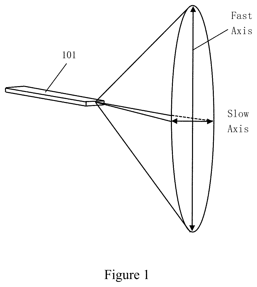
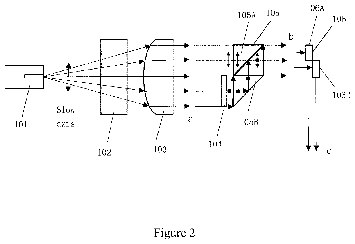
[0026]As shown in FIGS. 1 and 2, a semiconductor laser shaping device includes a semiconductor laser 101, (optionally) a fast axis collimating lens 102, a slow axis collimating lens 103, a half wave plate 104, a polarization beam combining prism 105, and a crawling prism group 106, which are sequentially disposed along an optical path.

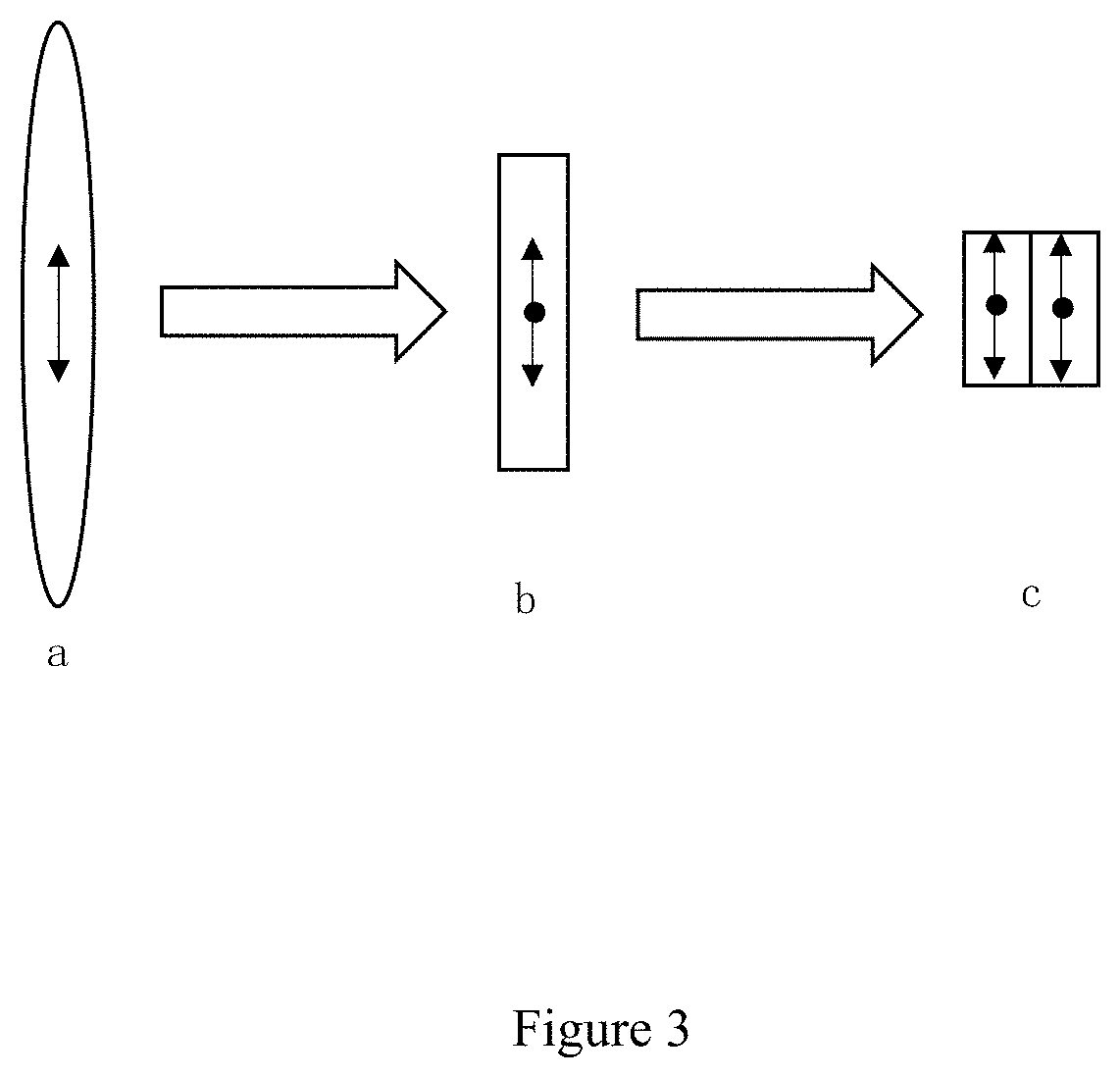
[0027]The laser beam emitted from the semiconductor laser 101 is collimated by the fast axis collimating lens 102 and the slow axis collimating lens 103 to produce a collimated laser beam at position (a) in FIG. 2. The polarization of the collimated laser beam is the in the plane of the slow axis as shown in FIG. 2. The fast axis collimating lens 102 and the slow axis collimating lens 103 can be implemented by cylindrical lenses that are aligned to focus the ...


PUM


Abstract

A semiconductor laser shaping device includes, along the light path of a semiconductor laser, a fast axis collimating lens, slow axis collimating lens, the half wave plate, a polarization beam combining prism, and a crawling prism group. The laser emitted by the semiconductor laser is collimated by a fast-axis collimating lens and then by a slow-axis collimating lens, and subsequently injected into a half wave plate and polarization beam combining prism, which compresses its spot size along the slow axis while keeping the spot size unchanged along the fast axis. The laser beam then passes through the crawling prism group, which shifts a portion of the light in the slow-axis direction to the fast-axis direction, which again compresses the light beam in the slow-axis direction. The device can reduce the beam size of a semiconductor laser in the slow-axis direction, reducing its beam parameter product and improving beam quality.

Description

TECHNICAL FIELD[0001]The present application relates to the field of optical technology, and in particular, to a semiconductor laser shaping device.BACKGROUND OF THE INVENTION[0002]Semiconductor lasers have the advantages of high electro-optical conversion efficiency, small size, high power, high reliability, etc., and thus have broad applications in the fields of laser ranging, pump laser, material processing, and biomedical treatment. On the other hand, a semiconductor laser having a large light-emitting area has a large spot size and a large divergence angle. It is difficult for an ordinary beam shaping system to effectively improve the beam quality of a slow-axis direction light of a semiconductor laser having a large light-emitting area. Therefore, in order to obtain a wider range of applications, it is necessary to adopt a beam shaping method to solve the problem of poor beam quality and low power density.[0003]In the application of semiconductor fiber-coupled lasers, there ar...

Claims


Application Information

Patent Timeline
IPC IPC(8): G02B27/09G02B27/28G02B27/30
CPCG02B27/0955G02B27/0916G02B27/30G02B27/0972G02B27/286G02B27/283H01S5/0071G02B5/045G02B27/0966
Inventor ZHANG, SHAOFENGDING, GUANGLEIYANG, JIANYANGHU, HAOCHENGZHANG, HUAPINGYAN, YAWEIWAN, RENLIANG
Owner FUJIAN HITRONICS PHOTOELECTRIC CO LTD
Why Eureka
Try Eureka