
Methods of utilizing low temperature solder assisted mounting techniques for package structures

Active Publication Date: 2021-09-16
INTEL CORP
View PDF0 Cites 0 Cited by
  • Summary
  • Abstract
  • Description
  • Claims
  • Application Information

AI Technical Summary

Benefits of technology

The patent text describes a problem of warping in microelectronic package structures, especially in thin microelectronic packages, due to differences in coefficients of thermal expansion between materials. The text describes various methods and structures for addressing this problem, including the use of a substrate with a specific type of material that provides structural support for the die or device, and the use of conductive interconnect structures to provide electrical communication between the die and the substrate or other die. The technical effects of the patent text include reducing warping in microelectronic package structures and improving the stability and reliability of the semiconductor manufacturing process.

Problems solved by technology

Warpage in microelectronic package structures, especially in thin microelectronic packages, can be a fabrication challenge for semiconductor manufacturers.
Differences in coefficients of thermal expansion (CTE) between various materials in the microelectronic package structures, such as differences between substrates and microelectronic die, for example, may contribute to such warpage, especially when the packaged die / device undergoes temperature cycling.

Method used


Image

  • Methods of utilizing low temperature solder assisted mounting techniques for package structures
  • Methods of utilizing low temperature solder assisted mounting techniques for package structures
  • Methods of utilizing low temperature solder assisted mounting techniques for package structures

Examples


example 1

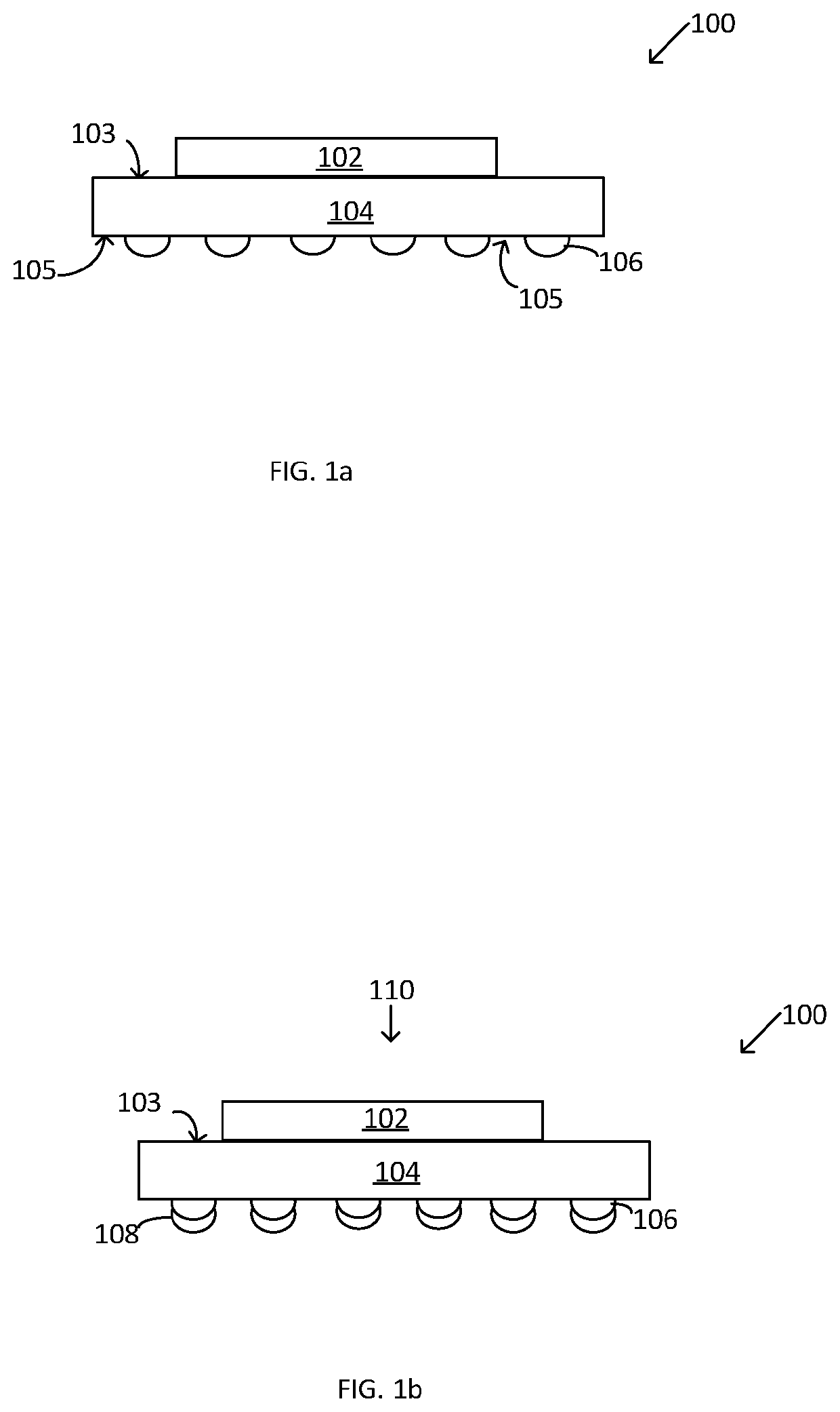
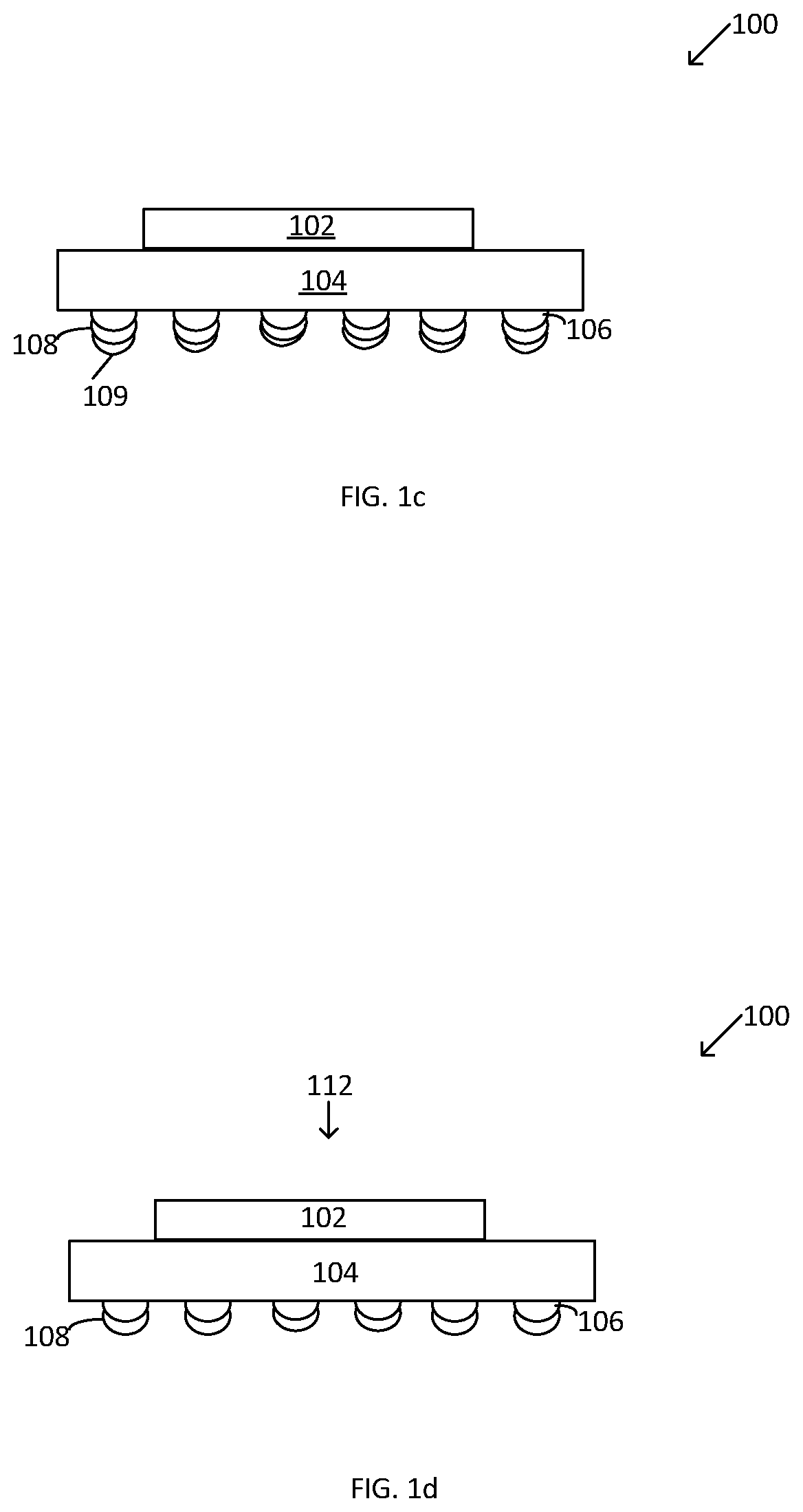
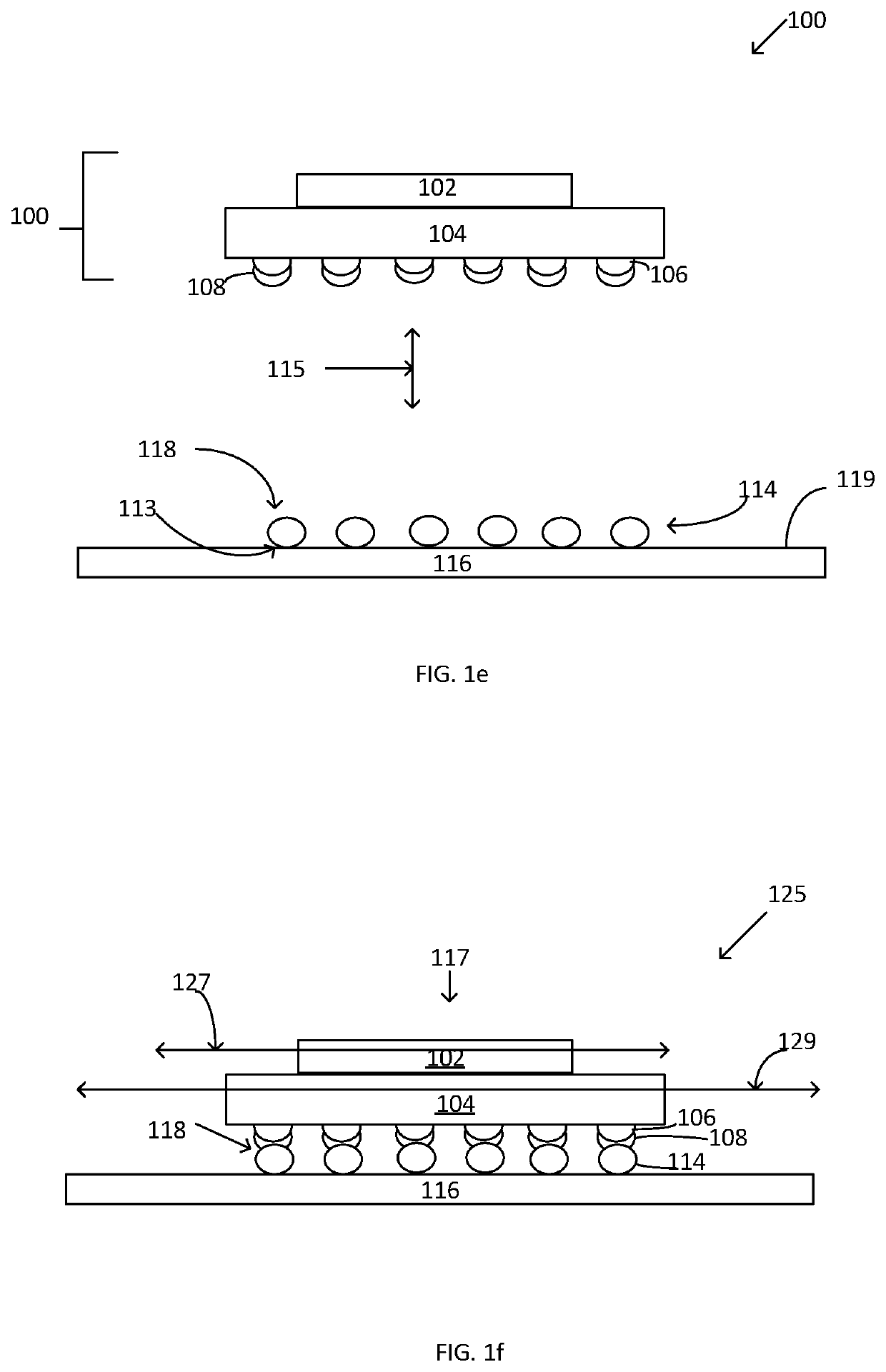
[0047 is a microelectronic package structure comprising a die on a first side of a first substrate. a first array of conductive interconnect structures is on a second side of the first substrate, wherein the first array of conductive interconnect structures comprises a high temperature solder material. A low temperature solder coating is disposed on at least a portion of the first array of conductive interconnect structures, wherein the low temperature solder coating comprises a low temperature solder alloying element, wherein the low temperature solder comprises a concentration of about 30 to about 50 percent of the low temperature solder ally element. The low temperature solder coating melts below about 200 degrees Celsius.

example 2

[0048 includes the structure of example 1 wherein a first side of a second array of conductive interconnect structures is disposed on the low temperature solder coating, wherein the second array of conductive interconnect structures comprise a high temperature solder material, wherein a melting temperature of the second array of conductive interconnect structures is above about 240 degrees Celsius.

example 3

[0049 includes the structure of example 2 wherein a second side of the second array of conductive interconnect structures is disposed on a second substrate.


PUM


Abstract

Methods / structures of joining package structures are described. Those methods / structures may include a device disposed on first side of substrate and an array of conductive interconnect structures disposed on a second side of the first substrate. The conductive interconnect structures of the array may comprise a solder material, wherein the solder material comprises a low temperature alloying element concentration of less than about 5 percent. A second substrate is coupled to the array of conductive interconnect structures.

Description

BACKGROUND OF THE INVENTION[0001]Warpage in microelectronic package structures, especially in thin microelectronic packages, can be a fabrication challenge for semiconductor manufacturers. Differences in coefficients of thermal expansion (CTE) between various materials in the microelectronic package structures, such as differences between substrates and microelectronic die, for example, may contribute to such warpage, especially when the packaged die / device undergoes temperature cycling.BRIEF DESCRIPTION OF THE DRAWINGS[0002]While the specification concludes with claims particularly pointing out and distinctly claiming certain embodiments, the advantages of these embodiments can be more readily ascertained from the following description of the invention when read in conjunction with the accompanying drawings in which:[0003]FIGS. 1a-1i represent cross-sectional views of structures according to embodiments.[0004]FIG. 2 represents a flow chart of a method according to embodiments.[0005...

Claims


Application Information

Patent Timeline
IPC IPC(8): H01L23/498H01L23/00H01L21/48
CPCH01L23/49816H01L23/49833H01L21/4857H01L21/4853H01L23/562H01L23/12H01L23/488H01L2924/14H01L2924/1432H01L2924/1433H01L2924/15192H01L2924/15311H01L2924/3511
Inventor KARHADE, OMKAR G.RARAVIKAR, NACHIKET R.SANE, SANDEEP B.
Owner INTEL CORP
Features
  • Generate Ideas
  • Intellectual Property
  • Life Sciences
  • Materials
  • Tech Scout
  • Unparalleled Data Quality
  • Higher Quality Content
  • 60% Fewer Hallucinations
Learn More