3-dimensional NAND flash memory device, method of fabricating the same, and method of driving the same

a technology of nand flash memory and 3D printing, applied in the field of semiconductor technology, can solve the problems of reducing the sensed margin of read operation, and achieve the effects of improving the reduction of read current, high degree of integration, and high speed

Active Publication Date: 2021-09-16
SK HYNIX INC +1
View PDF0 Cites 2 Cited by
  • Summary
  • Abstract
  • Description
  • Claims
  • Application Information

AI Technical Summary

Benefits of technology

[0016]According to embodiment of the present invention, a-3-dimensional NAND flash memory device includes a fixed charge region formed at an interface of the interlayer insulating layer adjacent to the information storing layer or in a portion of the information storing layer between the control gates; and an electrically doped region which is induced by the fixed charge region, and is formed on a partial surface of the semiconductor channel layer facing the fixed charge region. Therefore, it is possible to improve the reduction in read current. As a result, it is possible to provide a 3-dimensional NAND flash memory device having a high degree of integration, capable of driving at high speed and low power, and having a low occurrence of read errors.
[0017]Further, according to another embodiment of the present invention, a method of fabricating a 3-dimensional NAND flash memory device having the above-described advantages is provided.

Problems solved by technology

Thus, there is a problem that a sensing margin for read operation may be reduced.

Method used


Image

  • 3-dimensional NAND flash memory device, method of fabricating the same, and method of driving the same
  • 3-dimensional NAND flash memory device, method of fabricating the same, and method of driving the same
  • 3-dimensional NAND flash memory device, method of fabricating the same, and method of driving the same

Examples


Embodiment Construction

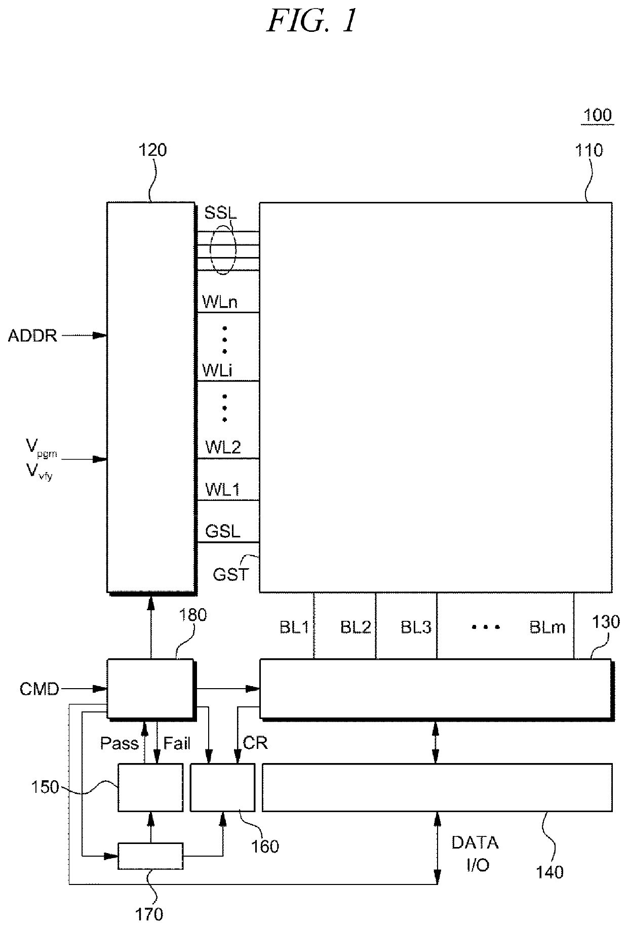
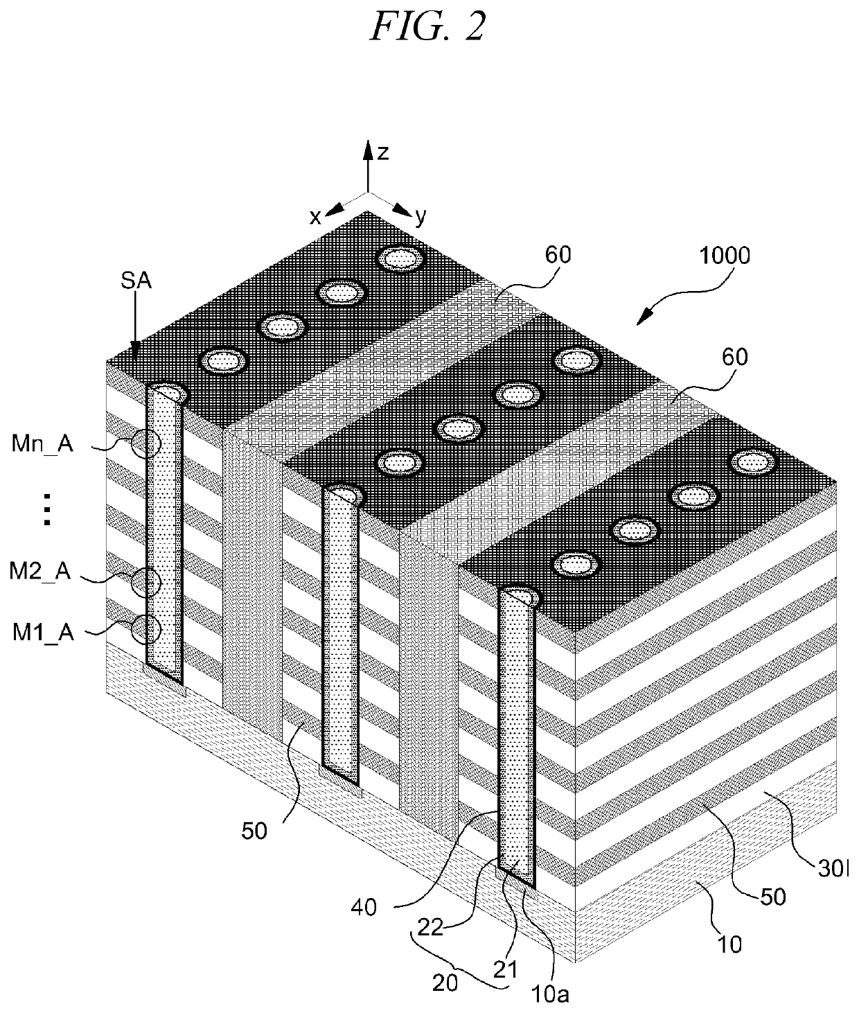
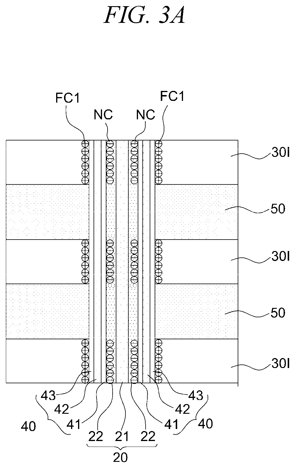
[0027]Hereinafter, the preferred embodiments of the present invention will be described in detail with reference to the accompanying drawings.

[0028]The embodiments of the present invention are provided to describe the present invention to those having a con non knowledge in the related art, and the following embodiments may be modified in various other forms, and the scope of the present invention is not limited to the following embodiments. Rather, these embodiments are provided to fully convey the spirit of the present invention to those skilled in the art.

[0029]The same reference numerals in the drawings refer to the same elements. Further, as used herein, the term, “and / or” includes any one and all combinations of one or more of the listed items.

[0030]The terminology used herein is used to describe a specific embodiment and is not intended to limit the present invention. As used herein, a singular form may include plural forms unless the context clearly indicates otherwise. Also...


PUM

PropertyMeasurementUnit
temperatureaaaaaaaaaa
positive voltageaaaaaaaaaa
driving voltageaaaaaaaaaa

Abstract

A 3-dimensional flash memory device and methods of fabricating and driving the same are provided. The device includes: a channel layer extending over a substrate in a first direction perpendicular to a surface of the substrate; an information storing layer extending along a sidewall of the channel layer in the first direction; control gates each surrounding, the channel layer, with the information storing layer between the channel layer and the control gates; an insulating layer being between the control gates in the first direction and separating the control gates from each other; a fixed charge region disposed at an interface of the insulating layer and the information storing layer or in a portion of the information storing layer between the control gates in the first direction; and a doped region induced by the fixed charge region and disposed at a surface of the channel layer facing the fixed charge region.

Description

CROSS-REFERENCES TO RELATED APPLICATION[0001]The present application claims the benefit of Korean patent application number 10-2020-0031945, filed on Mar. 16, 2020, which is herein incorporated by reference in its entirety.BACKGROUND OF THE INVENTION1. Field[0002]The present disclosure relates to semiconductor technology, and more particularly, to a 3-dimensional NAND flash memory device and a method of fabricating the same.2. Description of the Related Art[0003]As the demand for portable digital application devices such as digital cameras, smartphones, and tablet PCs is increasing and conventional hard disks are being replaced with solid-state drives (SSDs), the nonvolatile memory market is rapidly expanding. As the nonvolatile memory device, 3-dimensional NAND flash memory devices which may be highly integrated at low cost has been widely commercialized.[0004]The 3-dimensional NAND flash memory device may include a string selection transistor, a ground selection transistor, and ce...

Claims


Application Information

Patent Timeline
Patent Type & Authority Applications(United States)
IPC IPC(8): H01L27/11582H01L29/40H01L29/423H01L29/51H01L21/28H01L21/3105
CPCH01L27/11582H01L29/408H01L29/4234H01L21/3105H01L29/517H01L29/518H01L29/40117H01L29/513H10B41/27H10B43/27H01L29/792H01L29/66833H10B43/35
Inventor CHOI, WOO YOUNG
Owner SK HYNIX INC
Why Eureka
Try Eureka