
Test arrangement for testing high-frequency components, particularly silicon photonics devices under test

Active Publication Date: 2021-09-30
ADVANTEST CORP
View PDF0 Cites 1 Cited by
  • Summary
  • Abstract
  • Description
  • Claims
  • Application Information

AI Technical Summary

Benefits of technology

The patent describes a positioning apparatus for testing high-speed connectors on a device. The apparatus uses a movable cantilever arm to access and coupling with the device in a secure and easy way. The apparatus also includes coaxial connectors for blind-mating and non-core actual pogo pins for higher packaging density. The automatic test equipment has a flexible operation mode for testing components in a sequential or simultaneous manner. The technical effects of the invention include faster testing and higher data density.

Problems solved by technology

Devices under test can be highly complex setting challenging standards to automatic test equipment.
Specifically, photonic chips or hybrids thereof represent a particular challenge, since testing high-speed / high-frequency pins of a silicon photonics device under test at a wafer testing level in a high-volume production is only possible in separate process steps using different testing devices.
A big challenge is testing a die's electrical and photonics side simultaneously.
Different solutions have been developed to test silicon photonics chips but do not allow for testing high-speed / high-frequency pins of a silicon photonic part of a device under test in a reliable manner, since a failure coverage is very limited especially on the modulator part of the Photonics Circuit.

Method used


Image

  • Test arrangement for testing high-frequency components, particularly silicon photonics devices under test
  • Test arrangement for testing high-frequency components, particularly silicon photonics devices under test
  • Test arrangement for testing high-frequency components, particularly silicon photonics devices under test

Examples


Embodiment Construction

[0037]Equal or equivalent elements or elements with equal or equivalent functionality are denoted in the following description by equal or equivalent reference numerals even if occurring in different figures.

[0038]In the following description, a plurality of details is set forth to provide a more thorough explanation of embodiments of the present invention. However, it will be apparent to those skilled in the art that embodiments of the present invention may be practiced without these specific details. In other instances, well-known structures and devices are shown in block diagram form rather than in detail in order to avoid obscuring embodiments of the present invention. In addition, features of the different embodiments described herein after may be combined with each other, unless specifically noted otherwise.

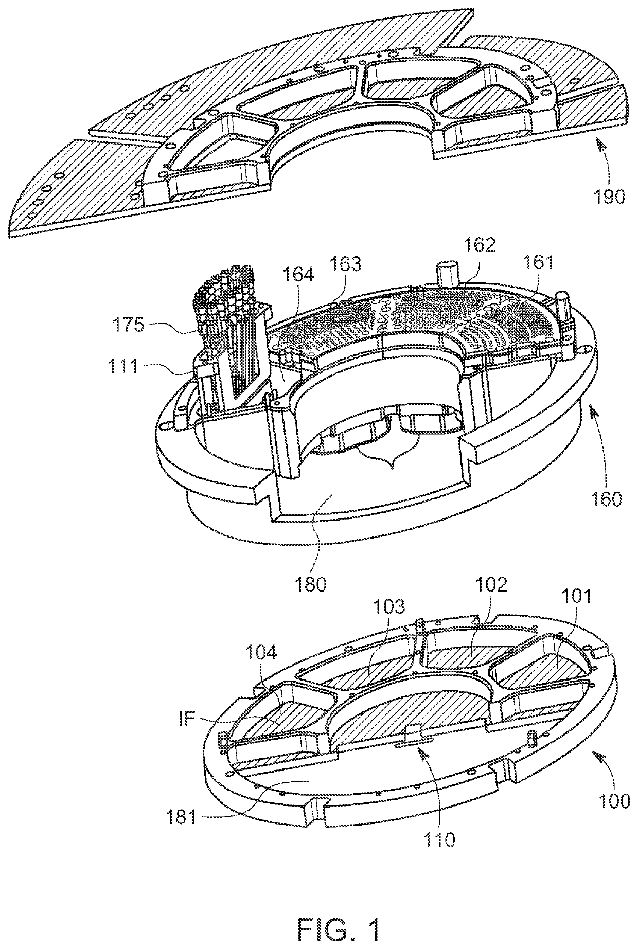
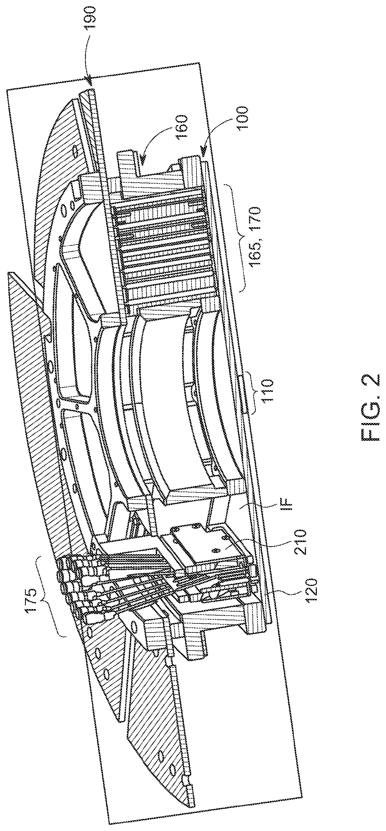
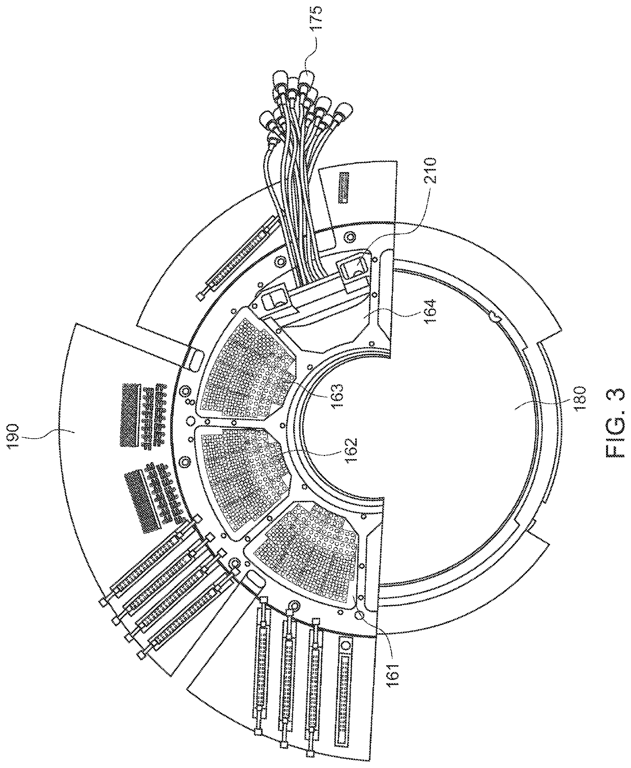
[0039]According to FIG. 1, an exploded view of a typical test fixture setup comprising a probe card 100, pogo tower 160 and the wafer probe interface of 190 according to an...


PUM


Abstract

The invention relates to a probe card (PC) for use with an automatic test equipment (ATE), wherein the probe card (PC) comprises a probe head (PH) on a first side thereof, and wherein the probe card (PC) is adapted to be attached to an interface (IF) and wherein the probe card (PC) comprises a plurality of contact pads on a second side in a region opposing at least a region of the interface (IF), arranged to contact a plurality of contacts of the interface (IF), and wherein the probe card (PC) comprises one or more coaxial connectors (CCPT) arranged to mate with one or more corresponding coaxial connectors (CCPT) of the interface (IF). The invention relates further to pogo tower (PT) for connecting a wafer probe interface (WPI) of an automatic test equipment with the probe card (PC).

Description

RELATED APPLICATION(S)[0001]The present application is a Continuation of PCT Application Number PCT / EP2020 / 058634, filed Mar. 26, 2020, which is incorporated herein by reference in its entirety.DESCRIPTIONTechnical Field[0002]Embodiments according to the invention relate to a probe card for use with an automatic test equipment, a pogo tower for connecting a wafer probe interface of the automatic test equipment with a probe card, the automatic test equipment and a method for testing a device under test using said automatic test equipment.Background of the Invention[0003]Automatic test equipment is widely used in the electronic manufacturing industry to test electronic components and systems after being fabricated. The device being tested is known as a device under test. Automatic test equipment quickly performs measurements and evaluates the test results. This is specifically necessary in the semiconductor industry where automatic test equipment can test a wide range of electronic de...

Claims


Application Information

Patent Timeline
IPC IPC(8): G01R1/067G01R1/073G01R31/28
CPCG01R1/06772G01R31/2834G01R1/07314G01R31/2851G01R1/073G01R1/0408G01R1/0416G01R31/2889G01R31/2884G01R31/311G01R31/2863G01R31/2808G01R1/0466G01R23/02G01R31/01
Inventor MOREIRA, JOSÉZHANG, ZHANWERKMANN, HUBERTPIZZA, FABIOMAZZUCCHELLI, PAOLO
Owner ADVANTEST CORP
Learn More