Method for forming precoat film and method for forming silicon-containing film

a technology of silicon-containing film and precoat, which is applied in the direction of coatings, chemical vapor deposition coatings, electric discharge tubes, etc., can solve the problems of less likely to obtain silicon-containing film of good quality, increased likelihood of metal contamination on the surface of the substrate,

Pending Publication Date: 2021-10-21
ASM IP HLDG BV
View PDF2 Cites 122 Cited by
  • Summary
  • Abstract
  • Description
  • Claims
  • Application Information

AI Technical Summary

Benefits of technology

[0009]According to the above embodiments of the present disclosure, for example, it is possible to provide a method for forming a precoat film and a method for producing a silicon-containing film, the methods being capable of suppressing a metal component contained in an inner wall surface of the chamber or a part disposed in the chamber from contaminating a substrate surface or a silicon-containing film formed on the substrate surface, even when the silicon-containing film is formed by the PECVD method.

Problems solved by technology

If a silicon-containing film is formed on a surface of a substrate by the PECVD method in a state in which a metal component remains in the chamber, likelihood that the surface of the substrate is contaminated with metal increases.
If a silicon-containing film is formed on the surface of the substrate contaminated with metal, a silicon-containing film with a good quality is less likely to be obtained.

Method used


Image

  • Method for forming precoat film and method for forming silicon-containing film
  • Method for forming precoat film and method for forming silicon-containing film
  • Method for forming precoat film and method for forming silicon-containing film

Examples


example

[0101]The Examples describe an embodiment in which a precoat film is formed using a plasma-enhanced atomic layer deposition (PEALD) method, and then a silicon-containing film is formed by a plasma-enhanced chemical vapor deposition (PECVD) method.

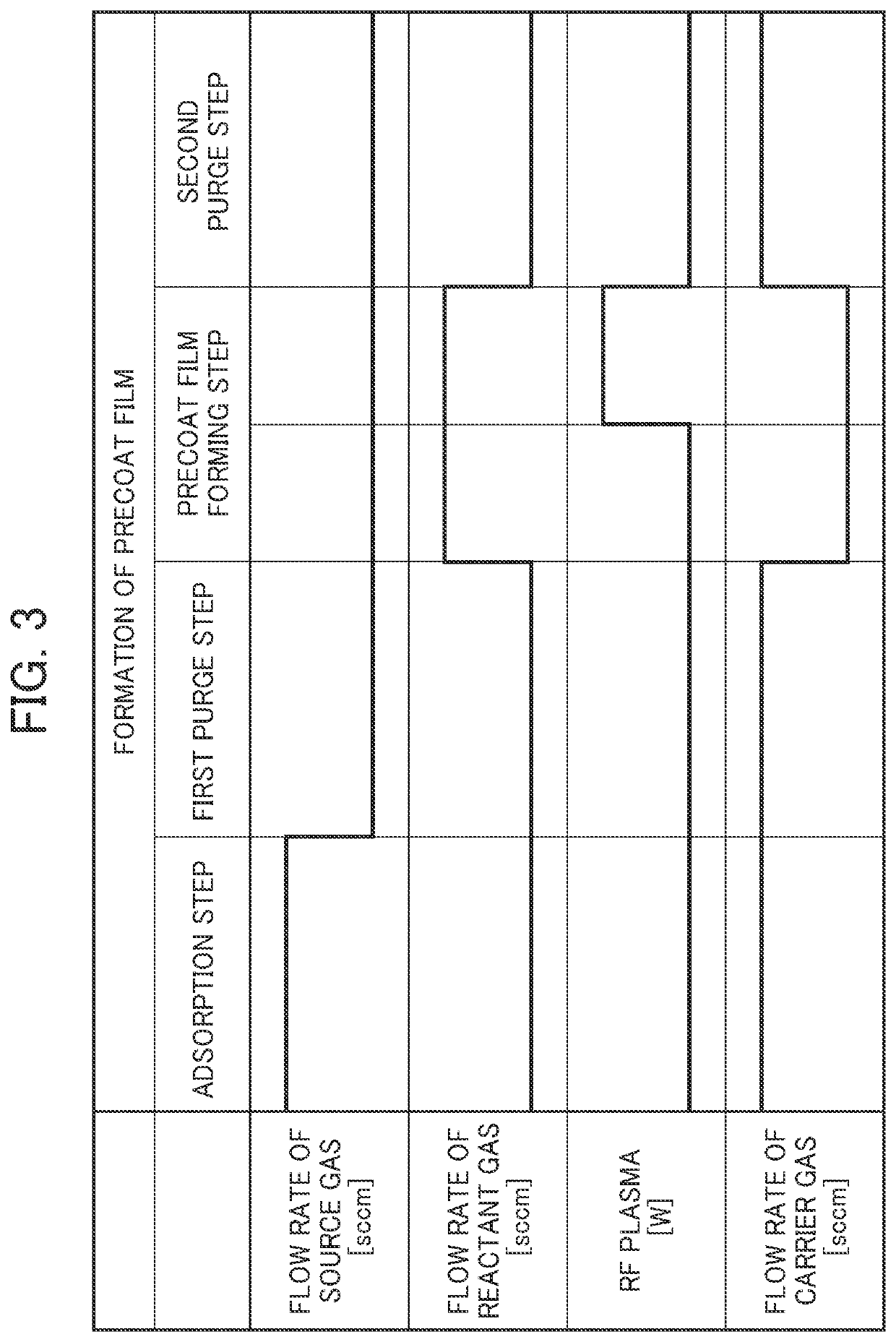
[0102][Precoat Film Forming Step]

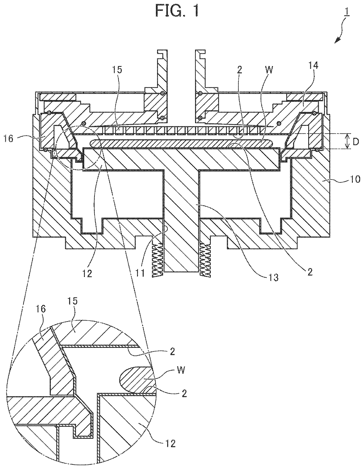
[0103]As shown in FIG. 1, a film forming device 1 which was used comprises a chamber 10 comprising a mounting table 12 with a diameter of 335 mm, which can mount a substrate Won a top surface thereof and function as a lower electrode, and a gas supply unit 14 with a diameter of 347 mm, which functions as an upper electrode. Here, as the mounting table 12, a mounting table made of aluminum nitride ceramics was used, and as the gas supply unit 14, a gas supply unit made of an aluminum (Al) alloy was used. Further, for some of the metal parts disposed in the chamber 10, parts made of an alloy containing copper (Cu) were used. Further, the size of a gap D between the mounting table 12 functioning as a lower elec...


PUM

PropertyMeasurementUnit
frequencyaaaaaaaaaa
temperatureaaaaaaaaaa
internal pressureaaaaaaaaaa

Abstract

A method for forming a precoat film on a metal surface in a chamber before forming a silicon-containing film having an identical composition system with that of the precoat film on a substrate in the chamber using a PECVD method, wherein the precoat film is formed using a PEALD method in which a first gas and a second gas are supplied into the chamber by shifting timing of supply, the PEALD method comprises an adsorption step comprising supplying the first gas into the chamber so that the source gas component adsorbs on the metal surface, a first purge step comprising discharging an excessive source gas component not adsorbed on the metal surface, and a precoat film forming step comprising supplying the second gas into the chamber and applying high-frequency power to generate plasma in the reactant gas component in the second gas.

Description

CROSS-REFERENCE TO RELATED APPLICATIONS[0001]This application claims the benefit of and priority to U.S. Provisional Application No. 63 / 010,357, filed on Apr. 15, 2020 in the United States Patent and Trademark Office, the disclosure of which is incorporated herein in its entirety by reference.BACKGROUND OF THE INVENTIONField of the Invention[0002]The present invention relates to a method for forming a precoat film on a metal surface in a chamber used in a plasma-enhanced chemical vapor deposition (PECVD) method, and a method of producing a silicon-containing film using the chamber in which the precoat film is formed.Related Art[0003]In the plasma-enhanced chemical vapor deposition (PECVD) method, a source gas and a reactant gas are supplied into a reaction vessel (chamber) in which a substrate is disposed, and plasma is generated to form a film on a surface of the substrate. This method is used for forming a film such as an insulating film on a substrate, such as a semiconductor waf...

Claims


Application Information

Patent Timeline
Patent Type & Authority Applications(United States)
IPC IPC(8): C23C16/02H01L21/02H01J37/32C23C16/455C23C16/34C23C16/40
CPCC23C16/0272H01L21/0217H01L21/02164H01L21/02274H01J37/3244H01J2237/3321C23C16/45536C23C16/345C23C16/402C23C16/45553H01J37/32183H01L21/0228C23C16/4404C23C16/45542C23C16/505
Inventor KUWANO, TAKERUSHIBA, EIICHIROHAMADA, TOSHIKAZUOTA, YOSHINORI
Owner ASM IP HLDG BV
Why Eureka
Try Eureka