
PMOSFET Source Drain

Active Publication Date: 2021-10-21
TAIWAN SEMICON MFG CO LTD
View PDF6 Cites 0 Cited by
  • Summary
  • Abstract
  • Description
  • Claims
  • Application Information

AI Technical Summary

Benefits of technology

The patent text describes a method for making a semiconductor device with a p-type multi-gate transistor that has a germanium channel. The technical effects of this invention include improved gate control, reduced off-state current, and reduced short-channel effects. The method involves using a combination of germanium and silicon materials to create a more efficient and effective device. The patent also includes cross-sectional views of the workpiece during the fabrication process. The invention is useful for improving the performance and reducing leakage of semiconductor devices.

Problems solved by technology

Such scaling down has also increased the complexity of processing and manufacturing ICs.
The fact that germanium has greater dielectric constant than silicon creates challenges.

Method used


Image

  • PMOSFET Source Drain
  • PMOSFET Source Drain
  • PMOSFET Source Drain

Examples


Embodiment Construction

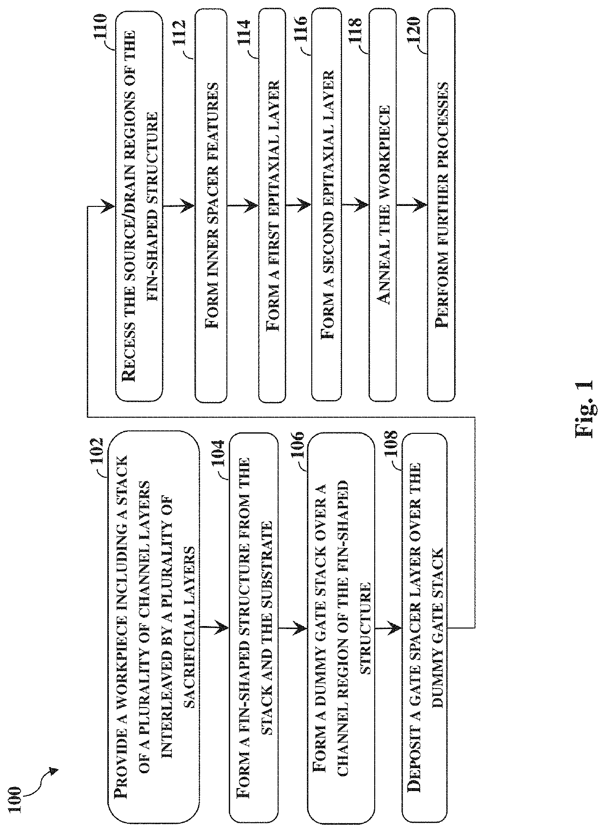
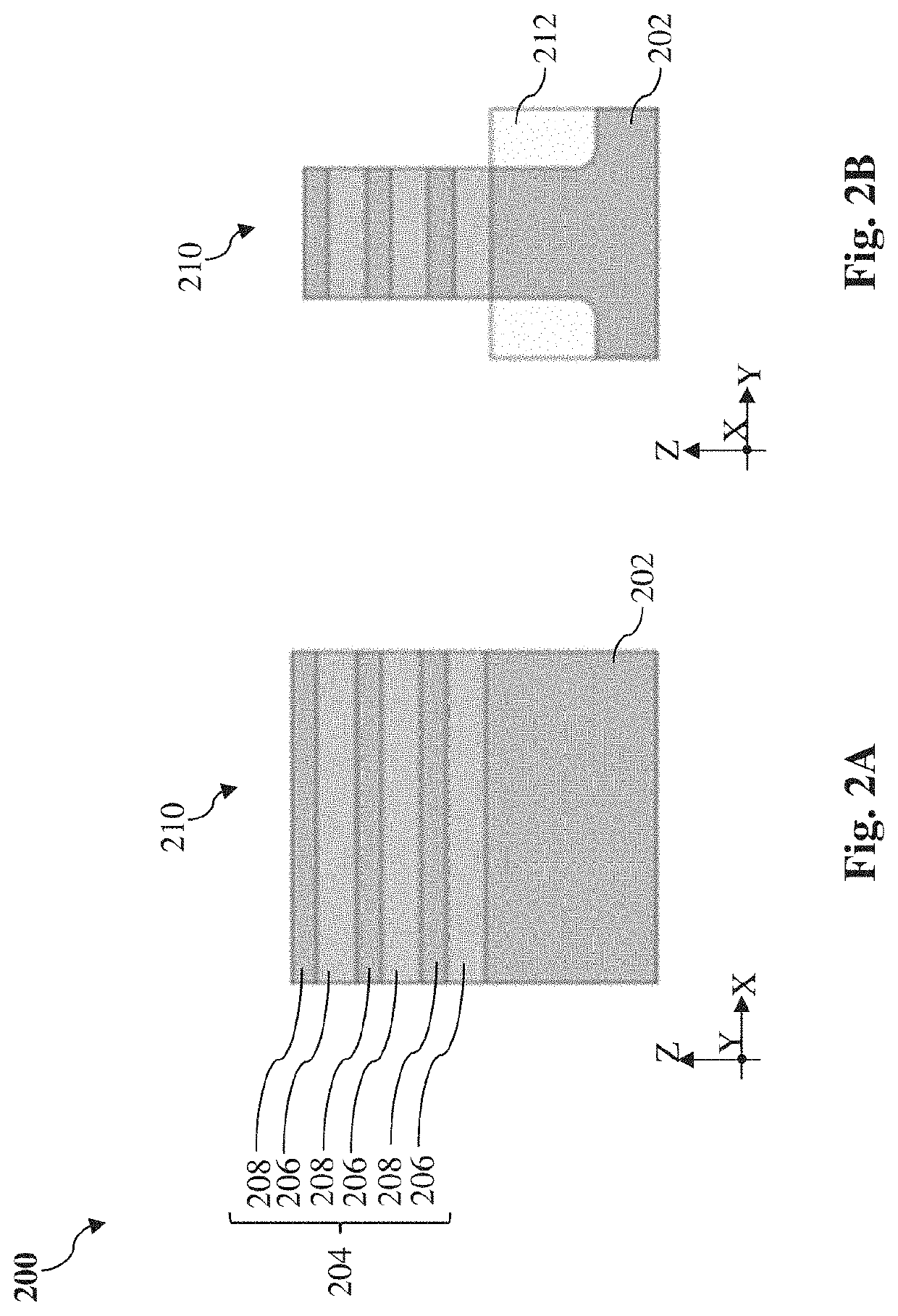
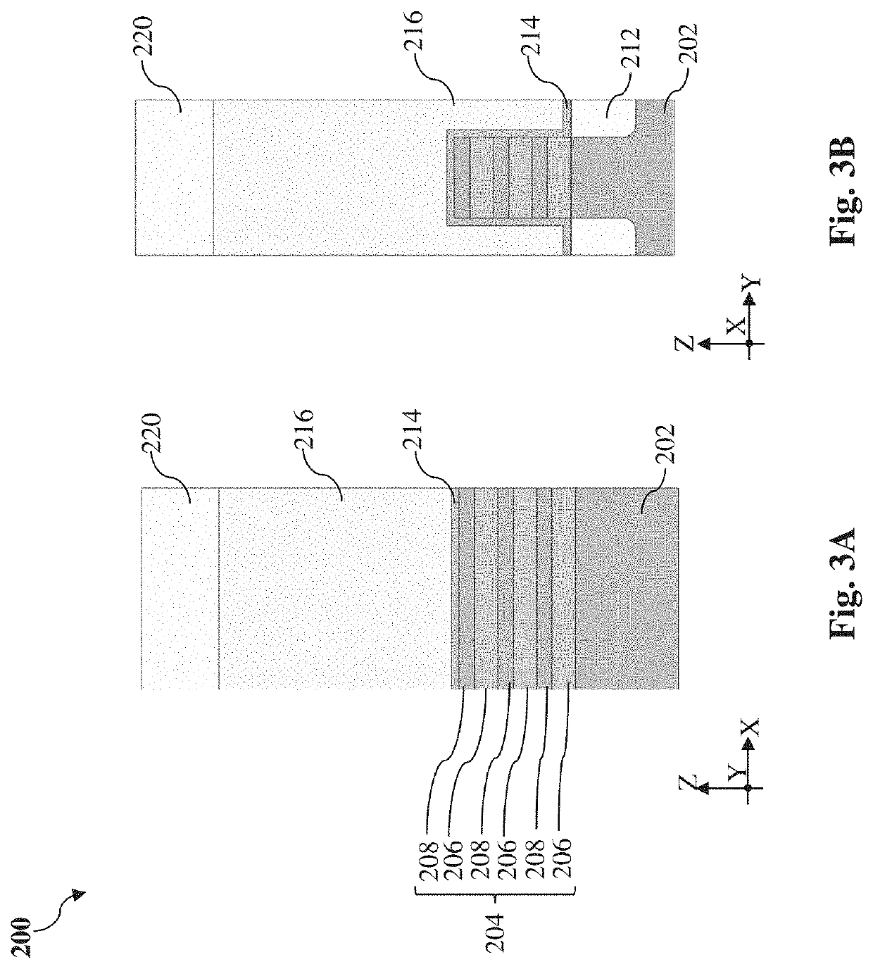
[0009]The following disclosure provides many different embodiments, or examples, for implementing different features of the provided subject matter. Specific examples of components and arrangements are described below to simplify the present disclosure. These are, of course, merely examples and are not intended to be limiting. For example, the formation of a first feature over or on a second feature in the description that follows may include embodiments in which the first and second features are formed in direct contact, and may also include embodiments in which additional features may be formed between the first and second features, such that the first and second features may not be in direct contact. In addition, the present disclosure may repeat reference numerals and / or letters in the various examples. This repetition is for the purpose of simplicity and clarity and does not in itself dictate a relationship between the various embodiments and / or configurations discussed.

[0010]F...


PUM


Abstract

A semiconductor device according to the present disclosure includes a first source / drain epitaxial feature and a second source / drain epitaxial feature each having an outer liner layer and an inner filler layer, a plurality of channel members extending between the first source / drain epitaxial feature and the second source / drain epitaxial feature along a first direction, and a gate structure disposed over and around the plurality of channel members. The plurality of channel members are in contact with the outer liner layer and are spaced apart from the inner filler layer. The outer liner layer comprises germanium and boron and the inner filler layer comprises germanium and gallium.

Description

PRIORITY DATA[0001]This application claims priority to U.S. Provisional Patent Application No. 63 / 010,834 filed on Apr. 16, 2020, entitled “PMOSFET SOURCE DRAIN” (Attorney Docket No. 2020-0759 / 24061.4175PV01), the entire disclosure of which is hereby incorporated herein by reference.BACKGROUND[0002]The semiconductor integrated circuit (IC) industry has experienced exponential growth. Technological advances in IC materials and design have produced generations of ICs where each generation has smaller and more complex circuits than the previous generation. In the course of IC evolution, functional density (i.e., the number of interconnected devices per chip area) has generally increased while geometry size (i.e., the smallest component (or line) that can be created using a fabrication process) has decreased. This scaling down process generally provides benefits by increasing production efficiency and lowering associated costs. Such scaling down has also increased the complexity of proc...

Claims


Application Information

Patent Timeline
IPC IPC(8): H01L29/167H01L29/165H01L29/78H01L29/66
CPCH01L29/167H01L29/165H01L29/7848H01L29/0669H01L29/66795H01L29/66545H01L29/66553H01L29/785H01L27/0924H01L21/823814H01L21/823821H01L29/66439H01L29/0673H01L29/42392H01L29/78696H01L29/66636H01L2029/7858
Inventor CHUNG, CHENG-TINGCHENG, KUAN-LUN
Owner TAIWAN SEMICON MFG CO LTD
Features
  • Generate Ideas
  • Intellectual Property
  • Life Sciences
  • Materials
  • Tech Scout
  • Unparalleled Data Quality
  • Higher Quality Content
  • 60% Fewer Hallucinations
Learn More