Method of fabrication of ai/ge bonding in a wafer packaging environment and a product produced therefrom

a technology of ai/ge bonding and packaging environment, which is applied in the direction of acceleration measurement using interia force, manufacturing tools, instruments, etc., can solve the problems of long-term reliability, drift of device performance, and high cost, and achieve the effect of reducing the number of defects, and reducing the cos

Active Publication Date: 2006-09-21
INVENSENSE
View PDF53 Cites 258 Cited by
  • Summary
  • Abstract
  • Description
  • Claims
  • Application Information

AI Technical Summary

Benefits of technology

[0017] A method of bonding two substrates to create a robust electrical and mechanical contact by using aluminum and germanium eutectic alloys is disclosed. An aluminum-germanium bond has the following unique combination of attributes: (1) it can form a hermetic seal; (2) it can be used to create an electrically conductive path between two substrates; (3) it can be patterned so that this conduction path is localized; (4) the bond can be made with the aluminum that is available as a standard foundry CMOS process; (5) this process is compatible with completely fabricated CMOS wafers as post process; (6) this process can provide for high density electrical interconnect; and (7) this process is highly controllable and provides for the smallest gap between two substrates. This has the significant advantage of allowing for wafer-level bonding or packaging without the addition of any additional process layers to the CMOS wafer.

Problems solved by technology

Although hybrid integration can provide vertical MEMS devices, the cost tends to be high, since manual processing steps are usually required, and because hybrid integration is typically performed on single devices.
However, most of these processes have been limited to providing protection of a sensitive feature from post process handling, such as sawing, die bonding, testing, package, etc.
These materials have disadvantages in that because they are organic, they tend to outgas and so are unsuitable for forming hermetic enclosures, and also they are susceptible to solvents, or moistures which can lead to problems with long term reliability and drift of a device's performance.
Additionally, they are insulating materials and so are incapable of forming a conductive path between two substrates.
Several major drawbacks are that frit glass does not provide for electrical interconnection between the MEMS and cover, to achieve a hermetic seal interface, minimum of 400 micron seal ring width is required which makes small MEMS devices, such as resonators and optical devices, much larger than otherwise.
Although these processes are capable of doing / creating? hermetic seals and electrical interface, achieving fine features, small gaps and water uniformity are / is very challenging and will result in yield losses.
Hence it is not possible to specify one or two micron gap controls between the MEMS and CMOS substrates using this bonding methodology.

Method used


Image

  • Method of fabrication of ai/ge bonding in a wafer packaging environment and a product produced therefrom
  • Method of fabrication of ai/ge bonding in a wafer packaging environment and a product produced therefrom
  • Method of fabrication of ai/ge bonding in a wafer packaging environment and a product produced therefrom

Examples


first embodiment

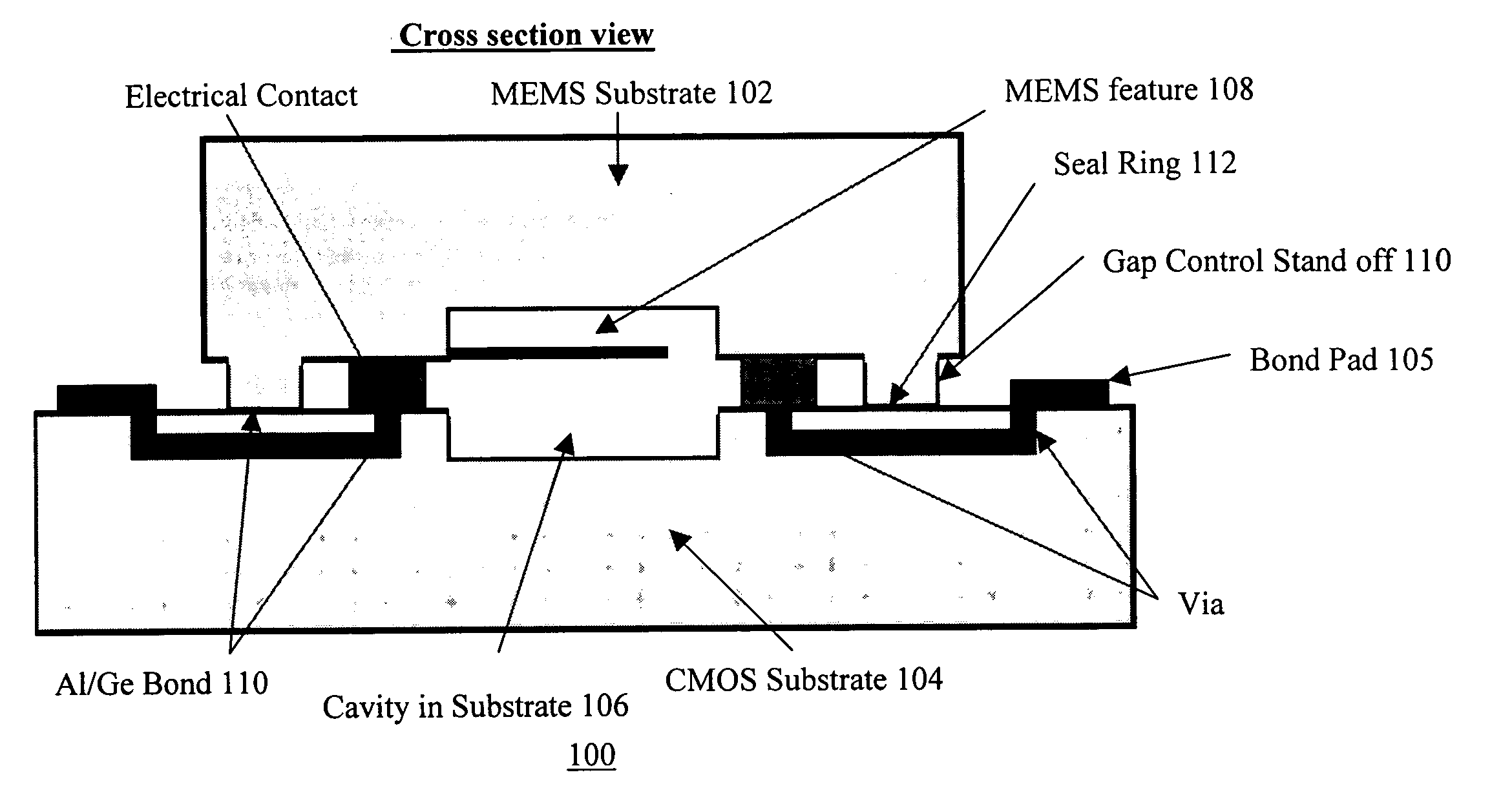
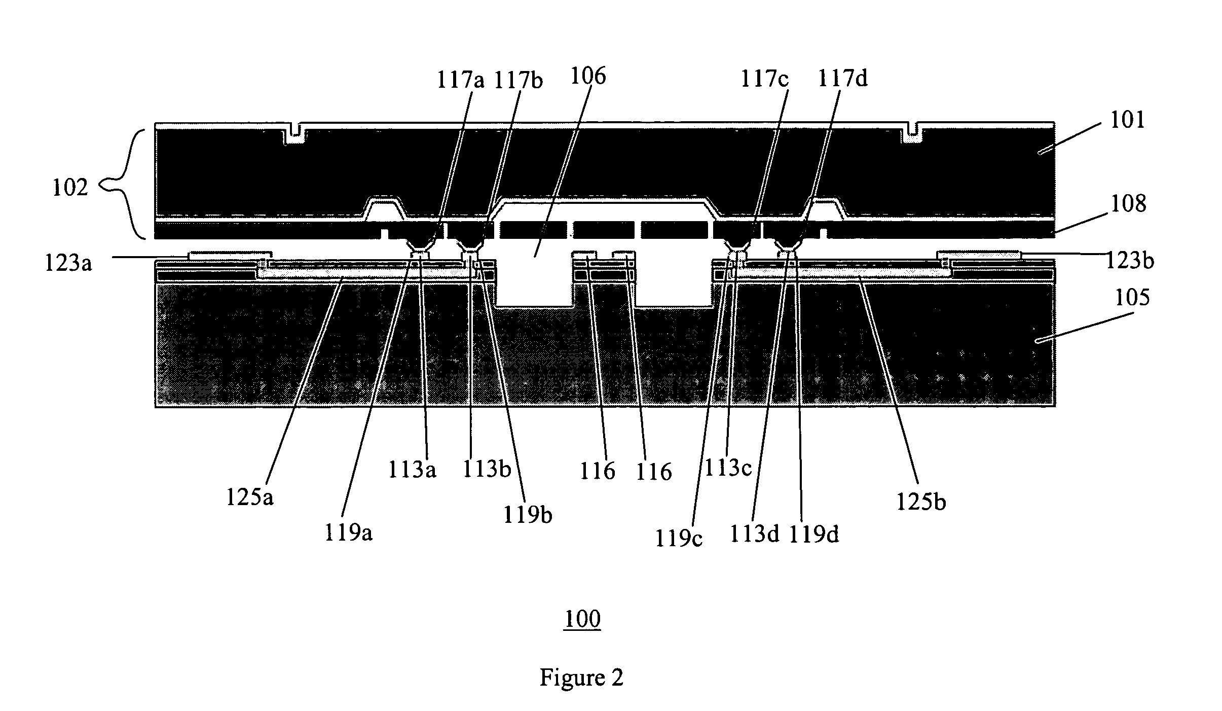
[0024] The following describes a preferred embodiment in accordance with the present invention. FIGS. 2A and 2B are cross sectional and top views of an assembly 100 in accordance with the present invention. Referring to the embodiment shown in FIG. 2A, a standard foundry CMOS wafer 104 which includes aluminum is bonded to a MEMS substrate 102 which includes germanium to provide an aluminum / germanium (Al / Ge) bond 110. In this embodiment, a cavity 106 is within the substrate 104. The CMOS substrate wafer 104 can be any substrate with patterned aluminum shown in FIG. 2B that is designed to interface with the MEMS substrate 102 to make for a complete functioning product. In addition, a plurality of aluminum contacts 116 are on the top of the CMOS substrate 104 which are coupled to bond pads 105 by interconnect 107. Vias 107 are provided in both the bond pads 105 and the aluminum contacts 116 to allow for electrical connection thereto. As an example, the substrate 104 can comprise only a...

second embodiment

[0025]FIGS. 3A and 3B are cross sectional and top views of an assembly in accordance with the present invention. The assembly 200 includes many of the same elements as assembly 100 of FIG. 2 and those elements have the same reference numerals. Additionally, the assembly 200 has via contacts 202 through the MEMS substrate 102′ and the gap control standoff 110′ to provide electric feedthrough of signals.

[0026] Another important feature of the substrate 104 is the availability of the multilayer metalization standard in CMOS foundries with chemical-mechanical-polishing of the oxide to make for a very planar metalized layer suitable for forming Al / Ge eutectic alloy with a germanium presence on the MEMS layer. The MEMS substrate 102 can be a silicon wafer or combination of silicon wafers assembled with all the MEMS features and functionalities including any type of preprocessed features.

[0027] In the preferred embodiment, the MEMS substrate on which the germanium has been patterned is a ...


PUM

PropertyMeasurementUnit
thickaaaaaaaaaa
thickaaaaaaaaaa
melting pointaaaaaaaaaa

Abstract

A method of bonding of germanium to aluminum between two substrates to create a robust electrical and mechanical contact is disclosed. An aluminum-germanium bond has the following unique combination of attributes: (1) it can form a hermetic seal; (2) it can be used to create an electrically conductive path between two substrates; (3) it can be patterned so that this conduction path is localized; (4) the bond can be made with the aluminum that is available as standard foundry CMOS process. This has the significant advantage of allowing for wafer-level bonding or packaging without the addition of any additional process layers to the CMOS wafer.

Description

FIELD OF THE INVENTION [0001] The present invention relates generally to wafer bonding and more particularly to a method and system of bonding in a wafer packaging environment. RELATED APPLICATIONS [0002] U.S. patent application Ser. No. 10 / 690,224, entitled “X-Y Axis Dual-Mass Tuning Fork Gyroscope with Vertically Integrated Electronics and Wafer-Scale Hermetic Packaging,” filed Oct. 20, 2003. [0003] U.S. patent application Ser. No. 10 / 691,472, entitled “Method of Making an X-Y Axis Dual-Mass Tuning Fork Gyroscope with Vertically Integrated Electronics and Wafer-Scale Hermetic Packaging,” filed Oct. 20, 2003. [0004] U.S. patent application Ser. No. 10 / 770,838, entitled “Vertically Integrated MEMS Structure,” filed Feb. 2, 2004. [0005] U.S. patent application Ser. No. 10 / 771,135, entitled “Vertical Integration of a MEMS Structure with Electronics in a Hermetically Sealed Cavity,” filed Feb. 2, 2004. BACKGROUND OF THE INVENTION [0006] MEMS technology has been under steady development...

Claims


Application Information

Patent Timeline
Patent Type & Authority Applications(United States)
IPC IPC(8): H01L29/84H01L21/00
CPCB81C1/00238B81C2203/0118B81C2203/035B81C3/001B81B3/0018B81C1/00269B81C2203/038B81C1/00H01L21/50H01L23/52H01L24/03H01L24/82H01L2224/02H01L2224/828H01L23/488B23K20/023B81B7/007B81B2203/0315B81B2207/012B81B2207/094B81C2203/0792H01L21/187
Inventor NASIRI, STEVEN S.FLANNERY, ANTHONY FRANCIS JR.
Owner INVENSENSE
Why Eureka
Try Eureka