Method of epitaxial germanium tin alloy surface preparation

a germanium tin alloy and surface preparation technology, applied in the direction of cleaning process and apparatus, cleaning using gases, chemical instruments and processes, etc., can solve the problems of less resistivity and higher threshold voltage, the size of transistor components is a challenge for engineers, and the electronic properties of the channel become less viabl

Active Publication Date: 2014-02-11
APPLIED MATERIALS INC
View PDF41 Cites 258 Cited by
  • Summary
  • Abstract
  • Description
  • Claims
  • Application Information

AI Technical Summary

Benefits of technology

[0010]In another embodiment, a method of preparing the surface of germanium tin (GeSn) or silicon germanium tin (SiGeSn) layers can include positioning a substrate with an exposed GeSn or SiGeSn layer in a processing chamber, flowing H2 into the chamber while maintaining a constant pressure, heating the chamber to a first temperature while maintaining the flow of H2, wherein the temperature can be higher than 450° C. and can be maintained for a short period of time that could be less than 1 minute, stopping the flow of H2 into the chamber, cooling the chamber to a second temperature which can be below 400° C., prior to depositing another layer on top of the cleaned GeSn or SiGeSn surface, where the overlayer can include Ge, doped Ge, a GeSn layer, a SiGeSn layer, a doped GeSn layer, a doped SiGeSn layer, an insulator, or a metal.

Problems solved by technology

As device geometries decline according to Moore's Law, the size of transistor components poses challenges to engineers working to make devices that are smaller, faster, use less power, and generate less heat.
For example, as the size of a transistor declines, the channel region of the transistor becomes smaller, and the electronic properties of the channel become less viable, with more resistivity and higher threshold voltages.
However, the mobility of germanium is not superior to strained silicon, unless the germanium is also strained.
However, during the formation and subsequent treatment of the GeSn layer, the surface can become oxidized or affected by other impurities, affecting the subsequent deposition of any overlayer.
Unlike silicon surfaces, germanium surfaces are not effectively passivated by oxide formation.
The formation of unstable germanium oxides under atmospheric conditions lead to point defects in the surface which can lead to defects in subsequently deposited layers.

Method used


Image

  • Method of epitaxial germanium tin alloy surface preparation
  • Method of epitaxial germanium tin alloy surface preparation
  • Method of epitaxial germanium tin alloy surface preparation

Examples


Embodiment Construction

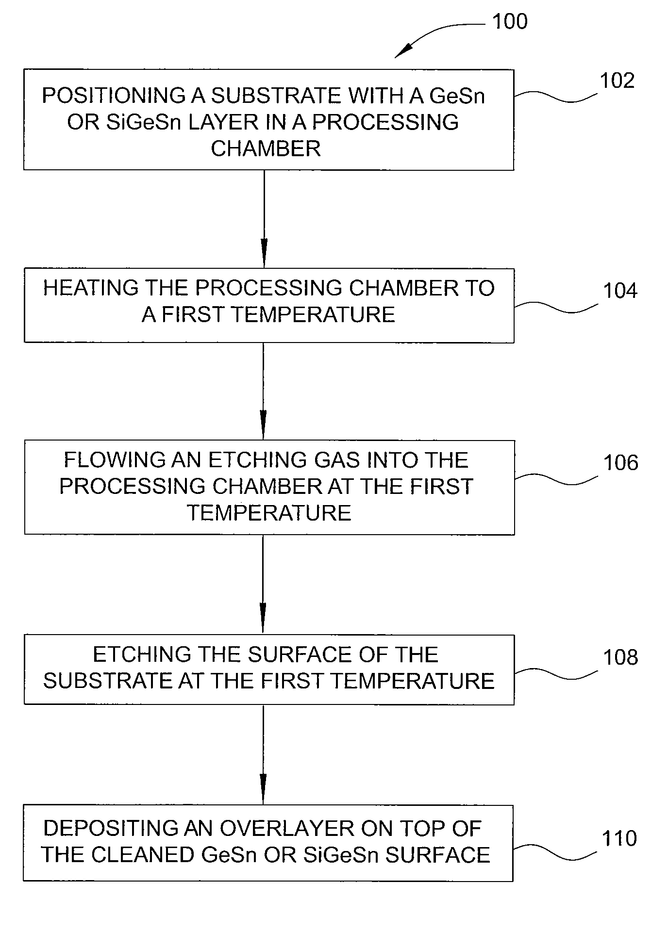
[0019]Methods for preparing the surface of germanium tin (GeSn) or silicon germanium tin (SiGeSn) layers for subsequent deposition are provided. The methods are described in more detail with reference to the figures below.

[0020]FIG. 1 is a flow diagram summarizing a method 100 according to one embodiment. A semiconductor substrate is positioned in a processing chamber at step 102. The semiconductor substrate may be any semiconductive material on which a stressor layer or an overlayer of any other function is to be formed. A silicon or germanium substrate on which a GeSn or SiGeSn layer is formed may be used in one example. The semiconductor substrate may have regions of oxide or surface contaminants formed on the GeSn or SiGeSn layer, which may be created at transfer steps between a vacuum environment and an ambient environment. For example, oxide may be formed and surface contaminants may be accumulated during the transfer steps between formation of a source / drain region and remova...


PUM

PropertyMeasurementUnit
temperatureaaaaaaaaaa

Abstract

Methods of preparing a clean surface of germanium tin or silicon germanium tin layers for subsequent deposition are provided. An overlayer of Ge, doped Ge, another GeSn or SiGeSn layer, a doped GeSn or SiGeSn layer, an insulator, or a metal can be deposited on a prepared GeSn or SiGeSn layer by positioning a substrate with an exposed germanium tin or silicon germanium tin layer in a processing chamber, heating the processing chamber and flowing a halide gas into the processing chamber to etch the surface of the substrate using either thermal or plasma assisted etching followed by depositing an overlayer on the substantially oxide free and contaminant free surface. Methods can also include the placement and etching of a sacrificial layer, a thermal clean using rapid thermal annealing, or a process in a plasma of nitrogen trifluoride and ammonia gas.

Description

BACKGROUND OF THE INVENTION[0001]1. Field of the Invention[0002]Technology described herein relates to the surface preparation of germanium tin (GeSn) or silicon germanium tin (SiGeSn) layers for subsequent deposition.[0003]2. Description of the Related Art[0004]Germanium was one of the first materials used for semiconductor applications such as CMOS transistors. Due to vast abundance of silicon compared to germanium, however, silicon has been the overwhelming semiconductor material of choice for CMOS manufacture. As device geometries decline according to Moore's Law, the size of transistor components poses challenges to engineers working to make devices that are smaller, faster, use less power, and generate less heat. For example, as the size of a transistor declines, the channel region of the transistor becomes smaller, and the electronic properties of the channel become less viable, with more resistivity and higher threshold voltages.[0005]Carrier mobility is increased in the sil...

Claims


Application Information

Patent Timeline
Patent Type & Authority Patents(United States)
IPC IPC(8): H01L21/3065H01L21/306
CPCH01L21/3065H01L21/02579H01L21/02576H01L21/02535H01L21/02532H01L21/02452H01L21/02661H01L21/0262H01L21/0245H01L21/306Y02E10/548
Inventor SANCHEZ, ERROL ANTONIO C.HUANG, YI-CHIAU
Owner APPLIED MATERIALS INC
Why Eureka
Try Eureka