Thin film transistor and manufacturing method thereof

a technology of thin film transistors and manufacturing methods, applied in transistors, semiconductor devices, electrical devices, etc., can solve the problems of easy undercuts and poor siox coverage, and achieve the effects of reducing the chance of oxidation, reducing the diffusion of copper ions, and improving the coverage of intermediate buffer layers

Active Publication Date: 2021-10-28
SHENZHEN CHINA STAR OPTOELECTRONICS SEMICON DISPLAY TECH CO LTD
View PDF0 Cites 0 Cited by
  • Summary
  • Abstract
  • Description
  • Claims
  • Application Information

AI Technical Summary

Benefits of technology

[0022]The present disclosure has the beneficial effects as follows: the materials of the intermediate buffer layer and the buffer layer are different, and the intermediate buffer layer is the ceramic material, wherein the intermediate buffer layer replaces silicon oxide, such as silicon nitride, with the ceramic material, which can avoid undercuts occurring to a silicon oxide single layer of the intermediate buffer layer, and improve the coverage of the intermediate buffer layer. Moreover, the diffusion of copper ions can be reduced, thereby reducing the chance of oxidation.

Problems solved by technology

In addition, the coverage of SiOx is poor, and undercuts easily occur.

Method used


Image

  • Thin film transistor and manufacturing method thereof
  • Thin film transistor and manufacturing method thereof

Examples


Embodiment Construction

[0025]Structure and technical means adopted by the present disclosure to achieve the above and other objects can be best understood by referring to the following detailed description of the preferred embodiments and the accompanying drawings. Furthermore, directional terms described by the present disclosure, such as upper, lower, front, back, left, right, inner, outer, side, longitudinal / vertical, transverse / horizontal, etc., are only directions by referring to the accompanying drawings, and thus the used directional terms are used to describe and understand the present disclosure, but the present disclosure is not limited thereto.

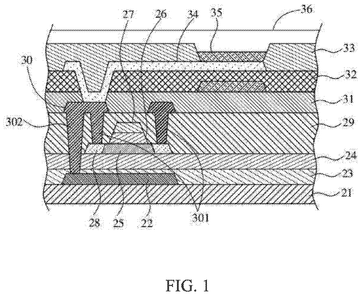
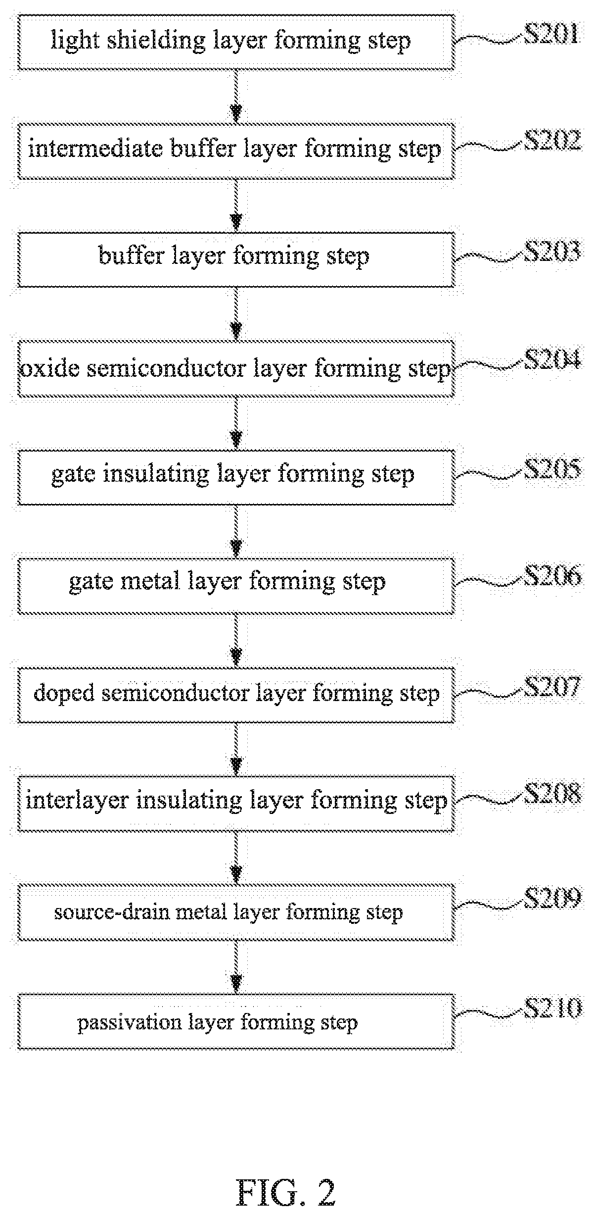
[0026]Referring to FIG. 1, a schematic view of a thin film transistor according to a preferred embodiment of the present disclosure is illustrated. The thin film transistor is a top-gate indium gallium zinc oxide (IGZO) thin film transistor. The thin film transistor includes a substrate 21, a light shielding layer 22, an intermediate buffer layer 23, a bu...


PUM

PropertyMeasurementUnit
thicknessaaaaaaaaaa
thicknessaaaaaaaaaa
electrical propertiesaaaaaaaaaa

Abstract

The present disclosure provides a thin film transistor and a manufacturing method thereof. The thin film transistor includes a substrate, a light shielding layer, an intermediate buffer layer, and a buffer layer, wherein the light shielding layer is formed on the substrate, the buffer layer is located above the substrate and the light shielding layer, the intermediate buffer layer is formed between the buffer layer and the light shielding layer, and the intermediate buffer layer is made of ceramic material.

Description

FIELD OF INVENTION[0001]The present disclosure relates to a thin film transistor and a manufacturing method thereof, and in particular, relates to a thin film transistor adopting indium gallium zinc oxide and a manufacturing method thereof.BACKGROUND OF INVENTION[0002]At present, oxide thin film transistors (Oxide TFT) are widely used in integrated circuits (IC) and image display device driving circuits for excellent performance thereof. As a channel for realizing charge transfer between the source and the drain of a TFT device, a channel layer of the field effect transistor is an important structure of the TFT device, and the structure and performance of the channel layer directly affect the electrical properties of the device product. A semiconductor thin film material may be selected as the channel layer, and a silicon-based semiconductor material and an oxide semiconductor material are known. An example of an oxide semiconductor material, indium gallium zinc oxide (IGZO).[0003]G...

Claims


Application Information

Patent Timeline
Patent Type & Authority Applications(United States)
IPC IPC(8): H01L29/786H01L21/02H01L29/66
CPCH01L29/78603H01L29/78633H01L29/7869H01L27/3262H01L21/02565H01L29/66969H01L21/02488H01L29/78606H01L29/0603H01L29/0684H01L29/66742H10K59/1213H10K59/126
Inventor LIU, FANGMEI
Owner SHENZHEN CHINA STAR OPTOELECTRONICS SEMICON DISPLAY TECH CO LTD
Why Eureka
Try Eureka