Supercharge Your Innovation With Domain-Expert AI Agents!

Polishing slurry composition and method for producing same

a technology of slurry and polishing, which is applied in the direction of polishing compositions with abrasives, other chemical processes, chemical instruments and processes, etc., can solve the problems of difficult to adjust the planarization degree, difficult to control dishing in a low stepped portion, and complicated surface structure of semiconductor devices. , to achieve the effect of enhancing the planarization degree, preventing dishing and scratches, and excellent polishing ra

Pending Publication Date: 2021-12-09
K C TECH
View PDF0 Cites 0 Cited by
  • Summary
  • Abstract
  • Description
  • Claims
  • Application Information

AI Technical Summary

Benefits of technology

The present patent discloses a polishing slurry composition that uses abrasive particles with controlled primary particle size and two or three types of dispersants with different charges. This composition prevents dishing and scratches during polishing, increases the polishing rate, and enhances planarization degree. Additionally, adjusting milling energy in the milling process controls the primary particle size, reduces the number of processes, and improves productivity. The "technical effects" of this composition and method include improved polishing performance, reduced defects, and improved productivity.

Problems solved by technology

As semiconductor devices become more diversified and highly integrated, finer pattern formation techniques are being used, and accordingly a surface structure of semiconductor devices becomes more complicated and a step height of surface films also becomes greater.
In a single-layered slurry generated by mixing an anionic polymer and an anionic copolymer, a high polishing rate and a selectivity in a high stepped portion may be realized, however, it is difficult to adjust a planarization degree and control dishing in a low stepped portion.
Also, there is a high probability of occurrence of scratches due to an intrinsic hardness of abrasive particles.

Method used


Image

  • Polishing slurry composition and method for producing same

Examples


examples 1 and 2

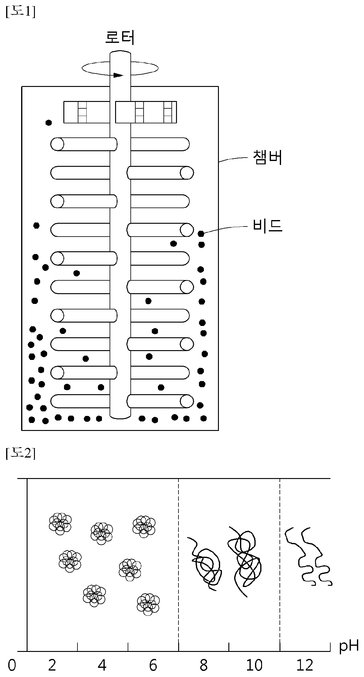
[0099 and Comparative Examples 1 and 2 were classified according to the milling conditions of Table 1 shown below, using the prepared polishing slurry composition.

TABLE 1Milling conditionsRotor milling speed (RPM)Bead filling ratio (%)Comparative70045Example 1Comparative63565Example 2Example 1110045Example 2110065

[0100]Silicon pattern wafers were polished according to Examples 1 and 2 and Comparative Examples 1 and 2 under the following polishing conditions.

[0101][Polishing conditions]

[0102]1. Polishing machine: AP-300 (manufactured by CTS)

[0103]2. Pad: K7 (manufactured by Rohm & Haas)

[0104]3. Polishing time: 60 seconds

[0105]4. Platen speed: 93

[0106]5. Spindle speed: 87

[0107]6. Flow rate: 250 ml / min

[0108]7. Wafer pressure: 3.0 psi

[0109]8. Used wafers:

[0110]PE-TEOS 20,000 Å, LP-Nitride 2,500 Å, P_Doped Poly 3,000 Å

[0111]STI Nitride Pattern (Nitride 1,000 Å, HDP 2,000 Å, Trench 1,200 Å)

[0112]Table 2 shows milling energy, characteristics of particles in the polishing slurry composition...


PUM

PropertyMeasurementUnit
primary particle diameteraaaaaaaaaa
zeta potentialaaaaaaaaaa

Abstract

The present disclosure relates to a polishing slurry composition and a method of producing the same. The polishing slurry composition according to one embodiment of the present disclosure includes: abrasive particles dispersed so as to have positively-charged particle surfaces; a first dispersant including a nonionic linear polymer; and a second dispersant including an anionic coiling polymer, wherein the polishing slurry composition satisfies the following Expressions 1 and 2: [Expression 1] 4≤log(milling energy) <5; and [Expression 2] 20% ≤Primary particle size reduction rate (%) <35%.

Description

TECHNICAL FIELD[0001]The present disclosure relates to a polishing slurry composition and a method of preparing the polishing slurry composition.BACKGROUND ART[0002]As semiconductor devices become more diversified and highly integrated, finer pattern formation techniques are being used, and accordingly a surface structure of semiconductor devices becomes more complicated and a step height of surface films also becomes greater. A chemical mechanical polishing (CMP) process is used as a planarization technique for removing a stepped portion of a specific film formed on a wafer in manufacturing of a semiconductor device. The CMP process is, for example, a process for removing an insulating film excessively formed for layer insulation, and is widely used as a process for planarizing an interlayer dielectric (ILD) and an insulating film for shallow trench isolation (STI) to insulate chips from each other and as a process for forming a metal conductive film, for example, a wiring, a conta...

Claims


Application Information

Patent Timeline
Patent Type & Authority Applications(United States)
IPC IPC(8): C09G1/02C09K3/14
CPCC09G1/02C09K3/14C09K3/1436C09K3/1409C09K3/1454
Inventor PARK, KWANG SOOHWANG, JUN HACHOI, SOO WANCHOI, NAK HYUN
Owner K C TECH
Features
  • R&D
  • Intellectual Property
  • Life Sciences
  • Materials
  • Tech Scout
  • Unparalleled Data Quality
  • Higher Quality Content
  • 60% Fewer Hallucinations
Learn More