
Automatic kerf offset mapping and correction system for laser dicing

Pending Publication Date: 2021-12-23
APPLIED MATERIALS INC
View PDF9 Cites 0 Cited by
  • Summary
  • Abstract
  • Description
  • Claims
  • Application Information

AI Technical Summary

Benefits of technology

The present patent discloses methods for determining scribing offsets in a hybrid laser scribing and plasma dicing process. This process involves forming a mask above a semiconductor wafer, patterning the mask and the wafer with a laser scribing process, and then removing the mask. The method also includes measuring the scribing offsets of the openings relative to the streets of the wafer. This can be useful in the singulation process, where the wafer is separated into individual dies. The patent also describes a semiconductor substrate with a device layer and trenches in the streets, where one or more of the trenches may be misaligned with the streets.

Problems solved by technology

One problem with either scribing or sawing is that chips and gouges can form along the severed edges of the dice.
In addition, cracks can form and propagate from the edges of the dice into the substrate and render the integrated circuit inoperative.
Chipping and cracking are particularly a problem with scribing because only one side of a square or rectangular die can be scribed in the direction of the crystalline structure.
Consequently, cleaving of the other side of the die results in a jagged separation line.
As a result of the spacing requirements, not as many dice can be formed on a standard sized wafer and wafer real estate that could otherwise be used for circuitry is wasted.
Furthermore, after cutting, each die requires substantial cleaning to remove particles and other contaminants that result from the sawing process.
Plasma dicing has also been used, but may have limitations as well.
For example, one limitation hampering implementation of plasma dicing may be cost.
A standard lithography operation for patterning resist may render implementation cost prohibitive.
Another limitation possibly hampering implementation of plasma dicing is that plasma processing of commonly encountered metals (e.g., copper) in dicing along streets can create production issues or throughput limits.

Method used


Image

  • Automatic kerf offset mapping and correction system for laser dicing
  • Automatic kerf offset mapping and correction system for laser dicing
  • Automatic kerf offset mapping and correction system for laser dicing

Examples


Embodiment Construction

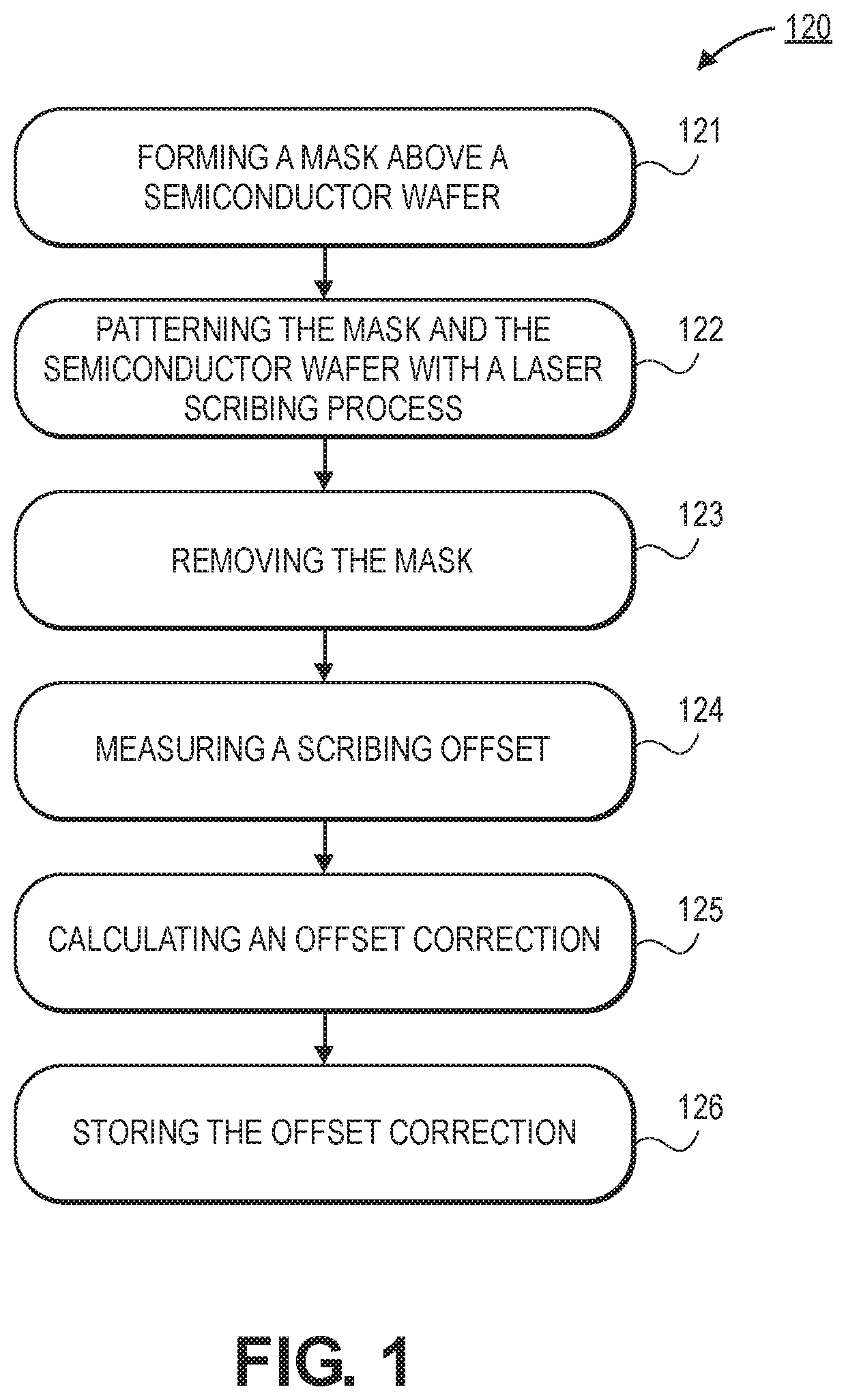
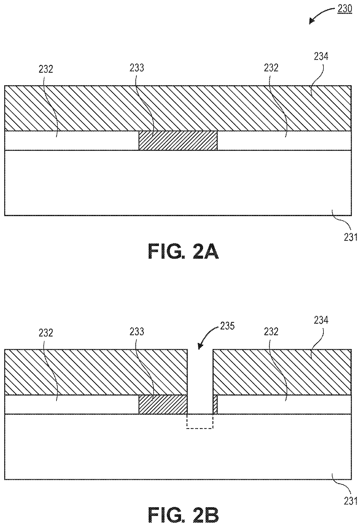
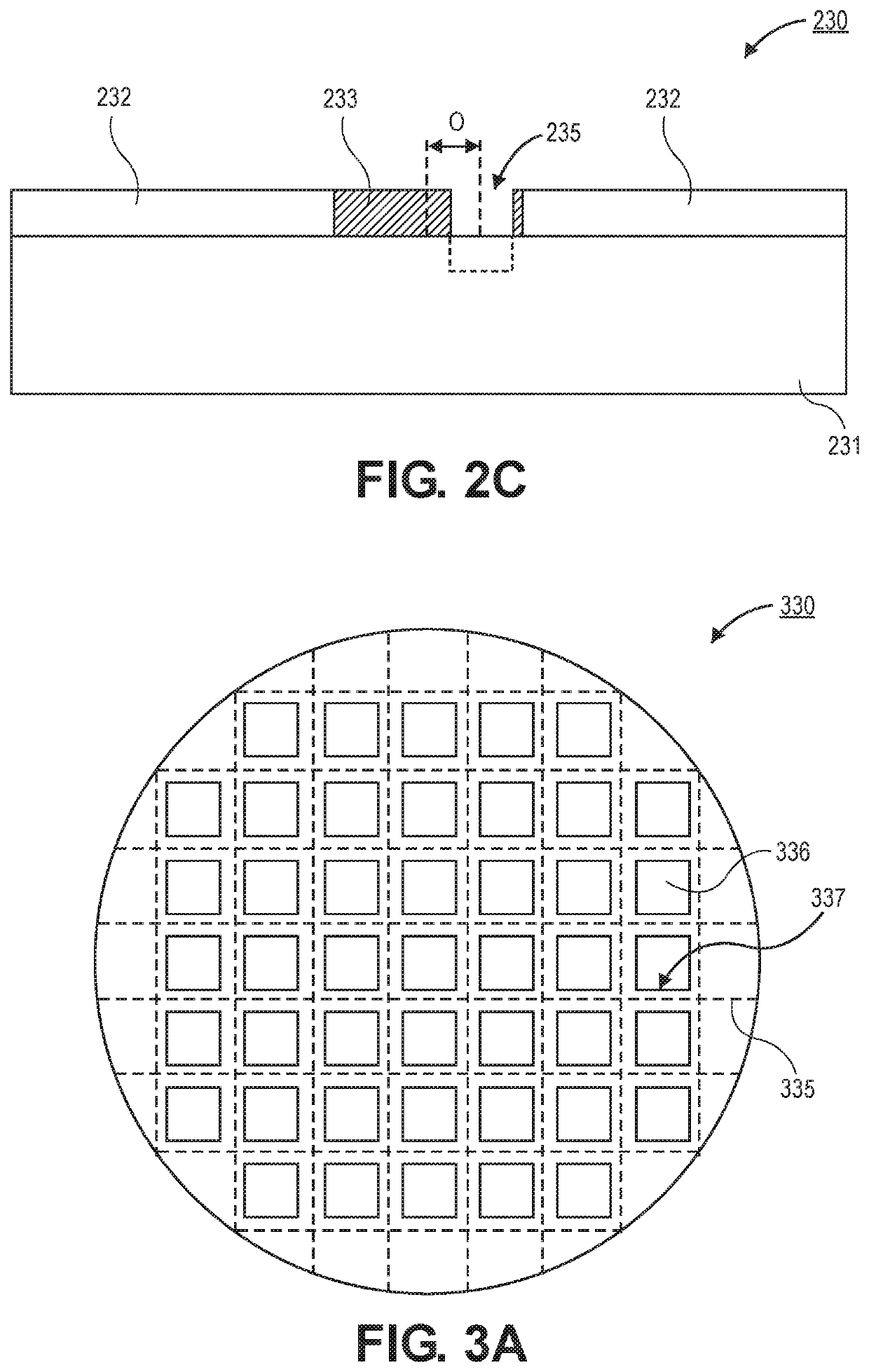
[0021]Methods of dicing semiconductor wafers, each wafer having a plurality of integrated circuits thereon, are described. In the following description, numerous specific details are set forth, such as offset mapping approaches for a hybrid laser and plasma dicing process, in order to provide a thorough understanding of embodiments of the present disclosure. It will be apparent to one skilled in the art that embodiments of the present disclosure may be practiced without these specific details. In other instances, well-known aspects, such as integrated circuit fabrication, are not described in detail in order to not unnecessarily obscure embodiments of the present disclosure. Furthermore, it is to be understood that the various embodiments shown in the Figures are illustrative representations and are not necessarily drawn to scale.

[0022]A hybrid wafer or substrate dicing process involving an initial laser scribe and subsequent plasma etch may be implemented for die singulation. The l...


PUM


Abstract

Embodiments of the present disclosure include methods of determining scribing offsets in a hybrid laser scribing and plasma dicing process. In an embodiment, the method comprises forming a mask above a semiconductor wafer. In an embodiment, the semiconductor wafer comprises a plurality of dies separated from each other by streets. In an embodiment, the method further comprises patterning the mask and the semiconductor wafer with a laser scribing process. In an embodiment, the patterning provides openings in the streets. In an embodiment, the method further comprises removing the mask, and measuring scribing offsets of the openings relative to the streets.

Description

BACKGROUND1) Field[0001]Embodiments of the present disclosure pertain to the field of semiconductor processing and, in particular, to methods of dicing semiconductor wafers, each wafer having a plurality of integrated circuits thereon.2) Description of Related Art[0002]In semiconductor wafer processing, integrated circuits are formed on a wafer (also referred to as a substrate) composed of silicon or other semiconductor material. In general, layers of various materials which are either semiconducting, conducting or insulating are utilized to form the integrated circuits. These materials are doped, deposited and etched using various well-known processes to form integrated circuits. Each wafer is processed to form a large number of individual regions containing integrated circuits known as dice.[0003]Following the integrated circuit formation process, the wafer is “diced” to separate the individual die from one another for packaging or for use in an unpackaged form within larger circu...

Claims


Application Information

Patent Timeline
IPC IPC(8): H01L21/78H01L21/027H01L21/3065
CPCH01L21/78H01L21/3065H01L21/0275
Inventor BALAKRISHNAN, KARTHIKPARK, JUNGRAETAN, ZAVIER ZAI YEONGABHINAND, SAIPAPANU, JAMES S.
Owner APPLIED MATERIALS INC
Learn More