Method of fabricating an electronic power module by additive manufacturing, and associated substrate and module

Active Publication Date: 2022-01-06
SAFRAN
View PDF9 Cites 0 Cited by
  • Summary
  • Abstract
  • Description
  • Claims
  • Application Information

AI Technical Summary

Benefits of technology

The invention is a substrate with a layer that helps increase its reliability and prevents it from bending or curving. This layer also provides electromagnetic shielding to protect the electronic components from external disturbances. This leads to a more stable and reliable electronic power module.

Problems solved by technology

Furthermore, the layer 8 of thermal interface material gives rise to thermal resistance that is not uniform, and that depends on the positioning of the semiconductor power components 3 on the power circuit, in particular if the circuit presents any planeness defect.
Furthermore, solutions for assembling the various layers 2a, 2b, 2c, and 5 having mutually different coefficients of thermal expansion make the electronic power module 1 sensitive to the phenomenon of thermal fatigue, thereby limiting the reliability of the electronic power module 1.
Nevertheless, as explained above, this layer 8 limits thermal dissipation between the semiconductor power components 3 and the heat dissipater 6 and gives rise to non-uniform thermal resistance that depends on the positioning of the semiconductor power components 3 on the power circuit.
It is therefore not possible to compensate for the flexing of the substrate 2 by increasing the thickness of the layer 8 of thermal interface material without further degrading heat dissipation within the electronic power module 1.

Method used


Image

  • Method of fabricating an electronic power module by additive manufacturing, and associated substrate and module
  • Method of fabricating an electronic power module by additive manufacturing, and associated substrate and module
  • Method of fabricating an electronic power module by additive manufacturing, and associated substrate and module

Examples


Embodiment Construction

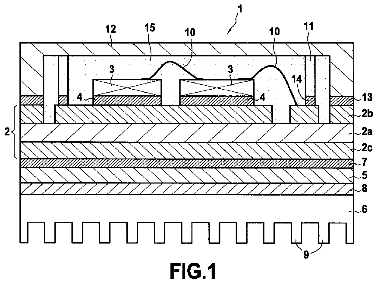
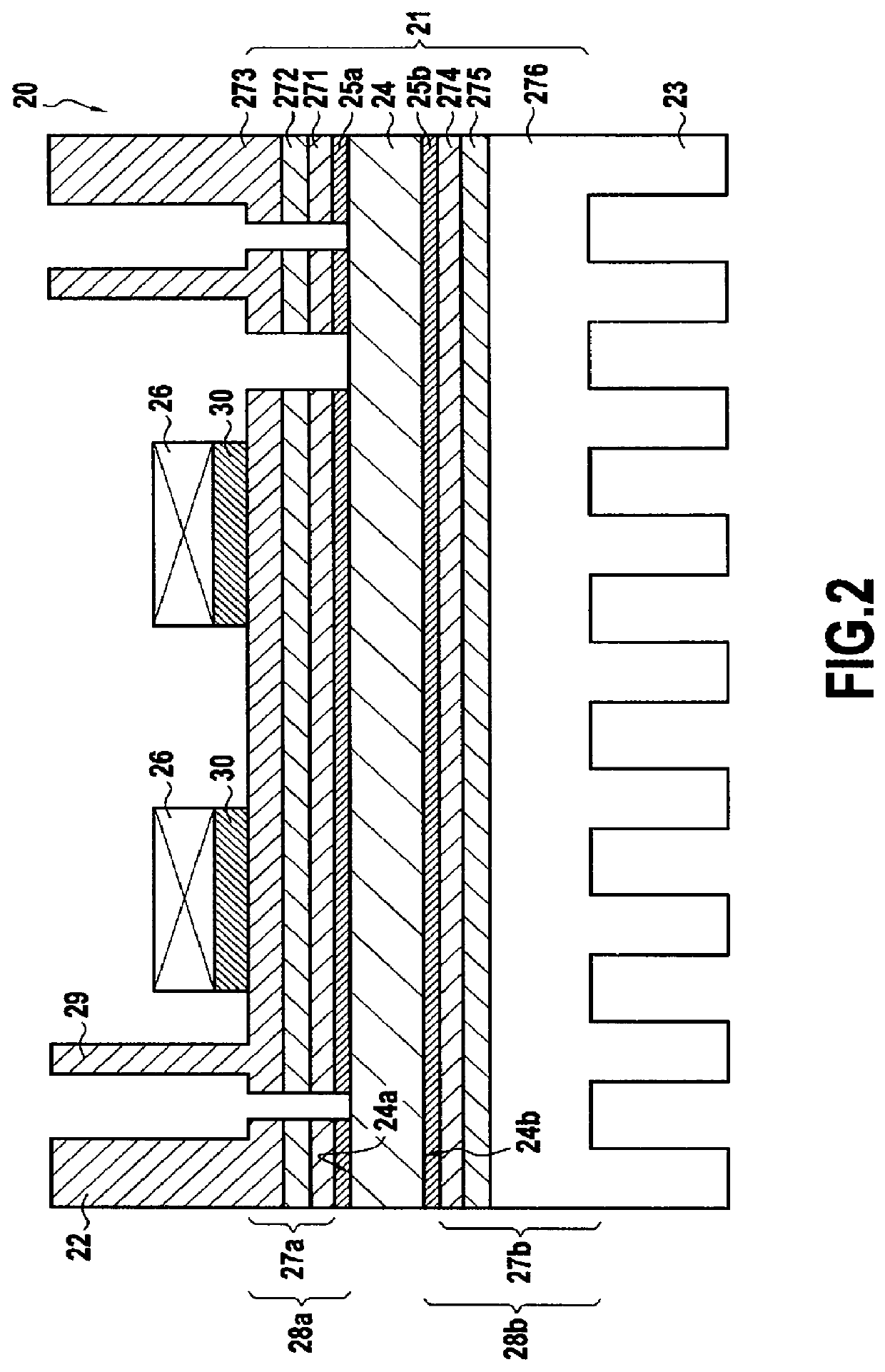
[0050]FIG. 2 is a diagram of an electronic power module 20 in an embodiment of the invention.

[0051]The electronic power module 20 comprises a substrate 21, a package 22, and a radiator 23.

[0052]The substrate 21 comprises an insulating plate 24 made of ceramic, e.g. Al2O3 or AlN, presenting a first face 24a and a second face 24b opposite from the first face 24a. The insulating plate 24 also has a first copper layer 25a and a second copper layer 25b deposited by silkscreen printing, respectively on the first face 24a and on the second face 24b of the insulating plate 24, which copper layers have been subjected to annealing. The first copper layer 25a forms electrically conductive tracks for connecting to electronic components 26, and the second copper layer 25b forms thermally conductive tracks for thermally coupling to the radiator 23.

[0053]The substrate 21 also has a first lay-up 27a of thermomechanical transition layers and a second lay-up 27b of thermomechanical transition layers....


PUM

PropertyMeasurementUnit
Temperature coefficient of resistanceaaaaaaaaaa
Coefficient of linear thermal expansionaaaaaaaaaa

Abstract

A method of fabricating an electronic power module by additive manufacturing, the electronic module including a substrate having an electrically insulating plate presenting opposite first and second faces, with a first metal layer arranged directly on the first face of the insulating plate, and a second metal layer arranged directly on the second face of the insulating plate. At least one of the metal layers is made by a step of depositing a thin layer of copper and a step of annealing the metal layer, and the method further includes a step of forming at least one thermomechanical transition layer on at least one of the first and second metal layers, the at least one thermomechanical transition layer including a material presenting a coefficient of thermal expansion that is less than that of the metal of the metal layer.

Description

CROSS-REFERENCE TO RELATED APPLICATIONS[0001]This application is a divisional of U.S. application Ser. No. 16 / 478,326, filed Jul. 16, 2019, which is the U.S. National Stage of PCT / FR2018 / 050024, filed Jan. 5, 2018, which in turn claims priority to French patent application number 1750381 filed Jan. 18, 2017. The content of these applications are incorporated herein by reference in their entireties.BACKGROUND OF THE INVENTION[0002]The invention relates to fabricating a substrate and an electronic power module.[0003]The present invention finds a particular application in the field of aviation where thermal stresses can be severe.[0004]Electronic power modules are included in the converters needed for electrifying propulsion and non-propulsion systems on board aircraft in order to convert electricity from the main network (115 volts alternating current (V AC), 230 V AC, 540 V direct current (DC) . . . ) into various forms (AC / DC, DC / AC, AC / AC, and DC / DC).[0005]FIG. 1 shows an example o...

Claims


Application Information

Patent Timeline
IPC IPC(8): A61K38/01A61K31/202A61K35/741A61K31/716A61K31/702A23L33/18A23L33/125A23L33/19A23L33/12A61K45/06H01L23/495
CPCA61K38/018A61K31/202A61K35/741A61K31/716A61K31/702A23L33/18A23V2002/00A23L33/19A23L33/12A61K45/06H01L23/49568H01L23/49513A23L33/125H01L23/3735H01L23/49822H01L21/4867H05K1/0271H05K1/0306H05K2201/0341H05K2201/068H05K2203/1344H01L2224/48137H01L2224/48472H01L2224/73265H01L2224/92247H01L2224/32225H01L2924/181H01L2224/48227H01L2924/00012H01L23/373
Inventor KHAZAKA, RABIHAZZOPARDI, STÉPHANEMARTINEAU, DONATIEN HENRI EDOUARD
Owner SAFRAN
Why Eureka
Try Eureka