Electronic component
a technology of electronic components and components, applied in the direction of inductances, fixed transformers or mutual inductances, inductances with magnetic cores, etc., can solve the problems of inability to reduce circuit resistance and circuit resistance fully, and achieve the effect of reducing circuit resistance, reducing circuit resistance, and reducing cross-sectional area of wiring
- Summary
- Abstract
- Description
- Claims
- Application Information
AI Technical Summary
Benefits of technology
Problems solved by technology
Method used
Image

Examples
first embodiment
[0025]Configuration
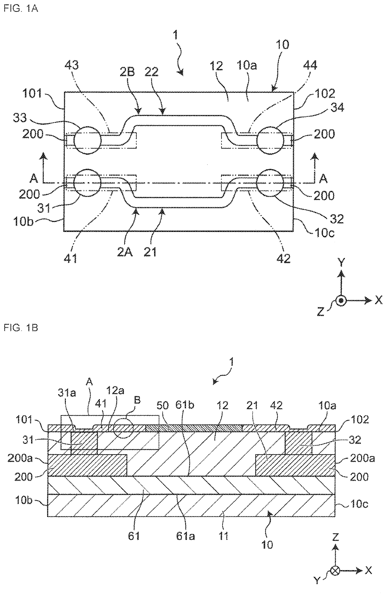
[0026]FIG. 1A is a perspective plan view of an electronic component according to a first embodiment. FIG. 1B is a sectional view taken along the line A-A of FIG. 1A.
[0027]The electronic component is, for example, an inductor component 1. The inductor component 1 is, for example, a surface-mount electronic component mounted on a circuit board mounted in an electronic device such as a personal computer, a DVD player, a digital camera, a TV, a mobile phone, or a car electronic system. The inductor component 1 is not limited to such a surface-mount electronic component and may be a board-mounted electronic component. The inductor component 1 is, for example, a component with substantially a cuboid shape as a whole. The shape of the inductor component 1 is not particularly limited and may be substantially a cylindrical shape, a polygonal column shape, a truncated cone shape, or a prismoid shape.
[0028]As illustrated in FIGS. 1A and 1B, the inductor component 1 includes ...
second embodiment
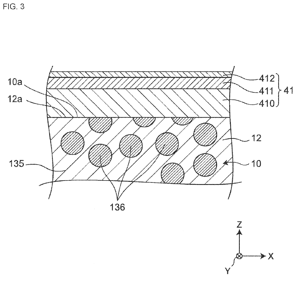
[0091]FIG. 5 is a partly enlarged view illustrating a second magnetic layer 12 and a metal film 410A in an electronic component 1A according to a second embodiment. The second embodiment differs from the first embodiment in the height of columnar wirings 31 to 34 relative to the upper surface of the second magnetic layer 12. This difference is described below. Other components are substantially the same as those in the first embodiment, are given the same reference numerals as those in the first embodiment, and will not be described in detail.
[0092]As illustrated in FIG. 5, in the second embodiment, a concave structure is used unlike a configuration according to the first embodiment in which the first principal surface 10a of the element body 10 has a flat structure. In FIG. 5, as well as in FIG. 2, a first cover layer 411 and a second cover layer 412 are omitted.
[0093]An end surface 31a of a first columnar wiring 31A is lower than the first principal surface 10a that is an outer su...
PUM
| Property | Measurement | Unit |
|---|---|---|
| thickness | aaaaa | aaaaa |
| size | aaaaa | aaaaa |
| size | aaaaa | aaaaa |
Abstract
Description
Claims
Application Information