Organic electroluminescent device, method of preparing conductive film material, and display panel

Pending Publication Date: 2022-01-27
WUHAN CHINA STAR OPTOELECTRONICS SEMICON DISPLAY TECH CO LTD
View PDF0 Cites 1 Cited by
  • Summary
  • Abstract
  • Description
  • Claims
  • Application Information

AI Technical Summary

Benefits of technology

[0026]Experiments have shown that the single-layered partially reduced graphene oxides have a transmittance of 97.7% and a thermal conductivity of 5000 W/m·K (about 10 times that of a metal material), so that the electrode made of such materials has excellent performance in terms of electrical and optical properties. Therefore, the organic electroluminescent device desc

Problems solved by technology

However, as resources of ITO raw materials become more and more scarce, manufacturing cost of display devices using ITO is becoming h

Method used


Image

  • Organic electroluminescent device, method of preparing conductive film material, and display panel
  • Organic electroluminescent device, method of preparing conductive film material, and display panel

Examples


embodiment 4

l

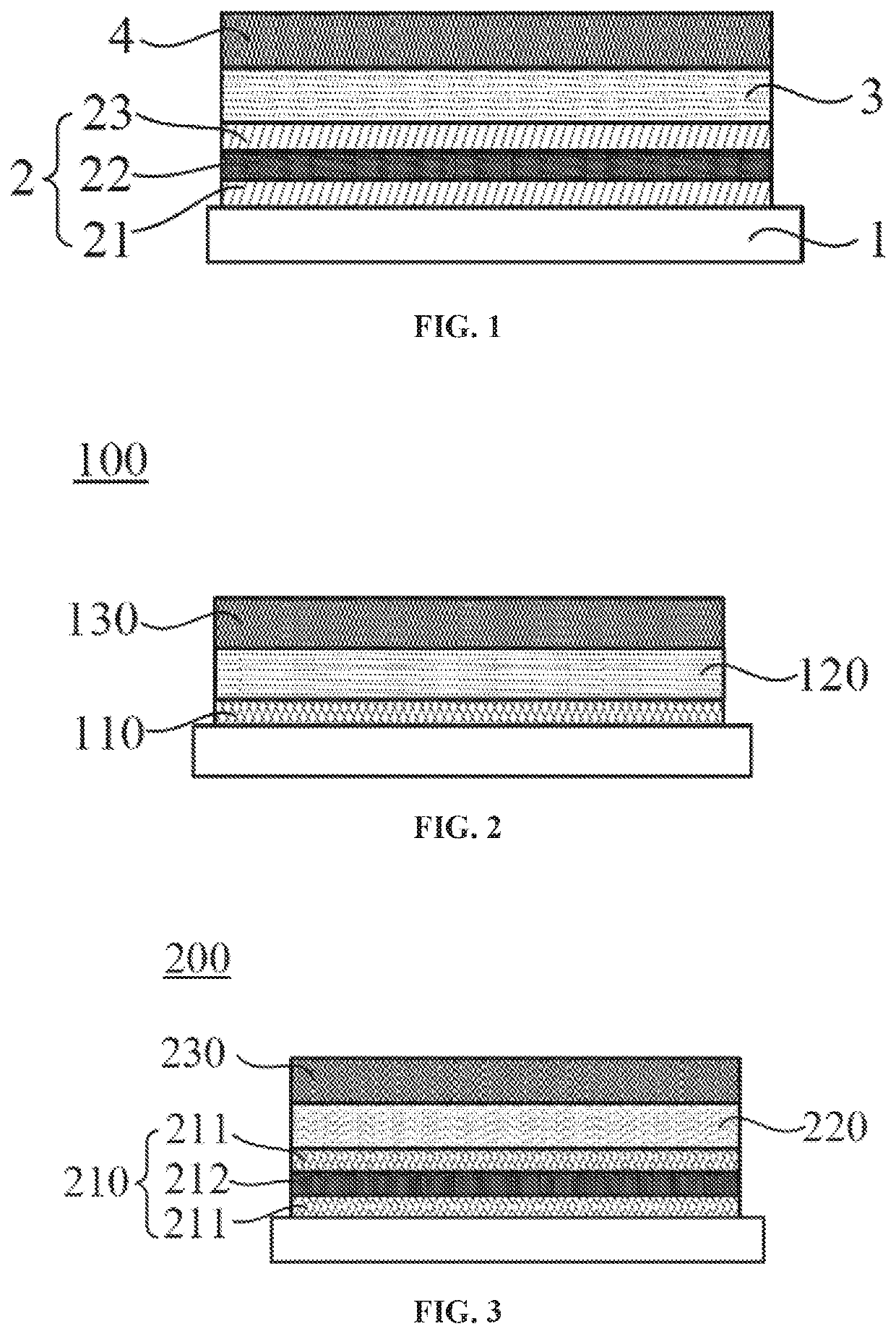
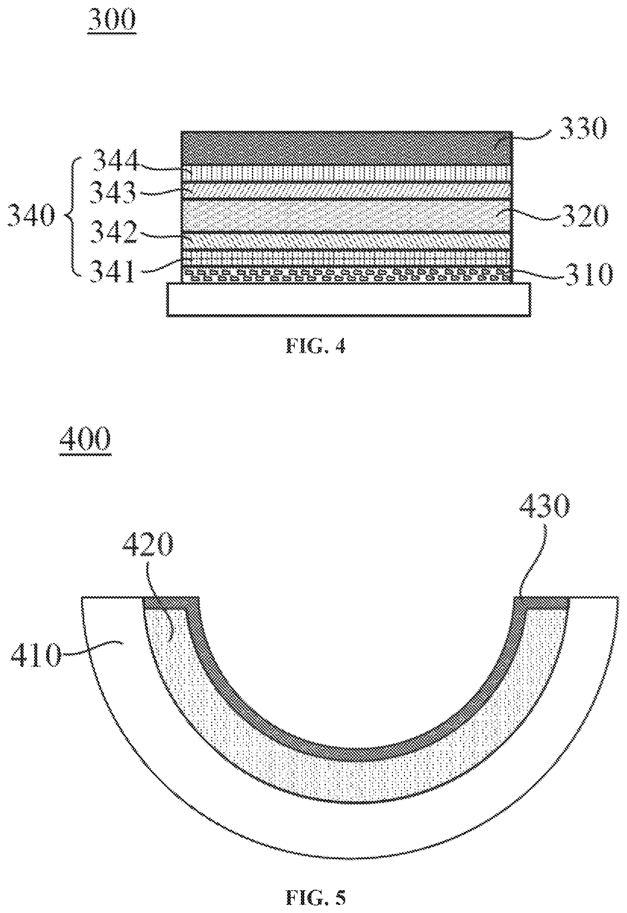
[0076]In the present embodiment, a display panel 400 is provided. As shown in FIG. 5, the display panel 400 includes a substrate 410 and a light-emitting device layer 420 formed on the substrate 410. Of course, the display panel 400 further includes other known structures such as a thin film encapsulation layer and a package cover. For example, as shown in FIG. 5, the display panel 400 further includes a conventional thin film encapsulation layer 430.

[0077]The light-emitting device layer 420 may include a plurality of organic electroluminescent devices 100 described in Embodiment 1, a plurality of the organic electroluminescent devices 200 described in Embodiment 2, or a plurality of the organic electroluminescent devices 300 described in Embodiment 3.

[0078]It can be understood by those skilled in the art that the substrate 410 can be selected from one of a glass substrate, a polyimide substrate, and a film substrate, and the structures prepared in a number of processes may be form...


PUM


Abstract

An organic electroluminescent device having an anode, wherein the anode comprises at least one first layer, the first layer being made of partially reduced graphene oxides.

Description

BACKGROUND OF INVENTIONField of Invention[0001]The present invention relates to a field of display technology, and in particular, to an organic electroluminescence device and a method of preparing a conductive film material used in the organic electroluminescence device and a display panel employing the organic electroluminescence device.Description of Prior Art[0002]Organic light-emitting diode (OLED) is considered to be the most promising new generation of display technology due to its excellent characteristics such as self-illumination, low energy consumption, wide viewing angles, rich colors, fast response times and capability of preparing a flexible screen.[0003]FIG. 1 is a schematic structural view of a conventional organic electroluminescent device. As shown in FIG. 1, the conventional organic electroluminescent device includes, in order from bottom to top, a substrate 1, an anode 2, an organic light-emitting layer 3, and a cathode 4. The substrate 1 is usually a hard-screen ...

Claims


Application Information

Patent Timeline
IPC IPC(8): C01B32/198
CPCC01B32/198H01L51/56H10K71/60H10K50/81H10K50/87H10K71/00C01P2006/60C01P2006/80H10K85/20H10K2102/311H10K50/84H10K2102/00
Inventor ZHANG, YUE
Owner WUHAN CHINA STAR OPTOELECTRONICS SEMICON DISPLAY TECH CO LTD
Why Eureka
Try Eureka