
Method for producing a microelectromechanical sensor and microelectromechanical sensor

a microelectromechanical and sensor technology, applied in the direction of fluid speed measurement, instruments, coatings, etc., can solve the problems of limiting the distance between the upper edge of the movable structure and the stop surface, damage or even destruction of the sensor, and the breakage of the fp bridge, so as to avoid the breakage of the functional fp bridge

Pending Publication Date: 2022-02-03
ROBERT BOSCH GMBH
View PDF0 Cites 0 Cited by
  • Summary
  • Abstract
  • Description
  • Claims
  • Application Information

AI Technical Summary

Benefits of technology

The present invention provides a method for producing stop structures on a cap wafer without causing damage to the functional bridges. The method includes applying a hard mask to the surface of the cap wafer, which prevents any material removal during subsequent etching processes. This in particular prevents overetching that could reduce the height of the stop surface.

Problems solved by technology

This results in a limiting factor for the distance between the upper edge of the movable structure and the stop surface; in particular, if the distance is too large, it can occur that the functional FP bridge impacts from below against solid structures of the sensor wafer before the movement of the stop surface is caught.
The impact can result in breakages of the FP bridge that may damage or even destroy the sensor.
In such structures, there is the problem that the FP bridge can suffer damage due to impacts against an immovable structure of the sensor wafer.
While, when there are large excursions of the movable structure, the substructures can be stopped by mechanical contact with one or more stop structures, such an impact of the FP bridge potentially causes damage to or destruction of the bridge, and therefore has to be avoided.

Method used


Image

  • Method for producing a microelectromechanical sensor and microelectromechanical sensor
  • Method for producing a microelectromechanical sensor and microelectromechanical sensor
  • Method for producing a microelectromechanical sensor and microelectromechanical sensor

Examples


Embodiment Construction

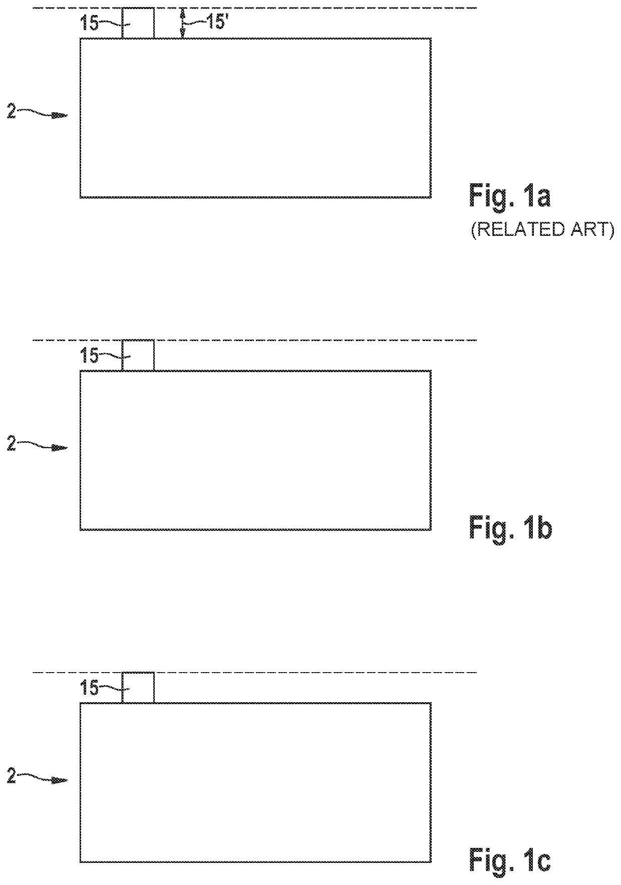
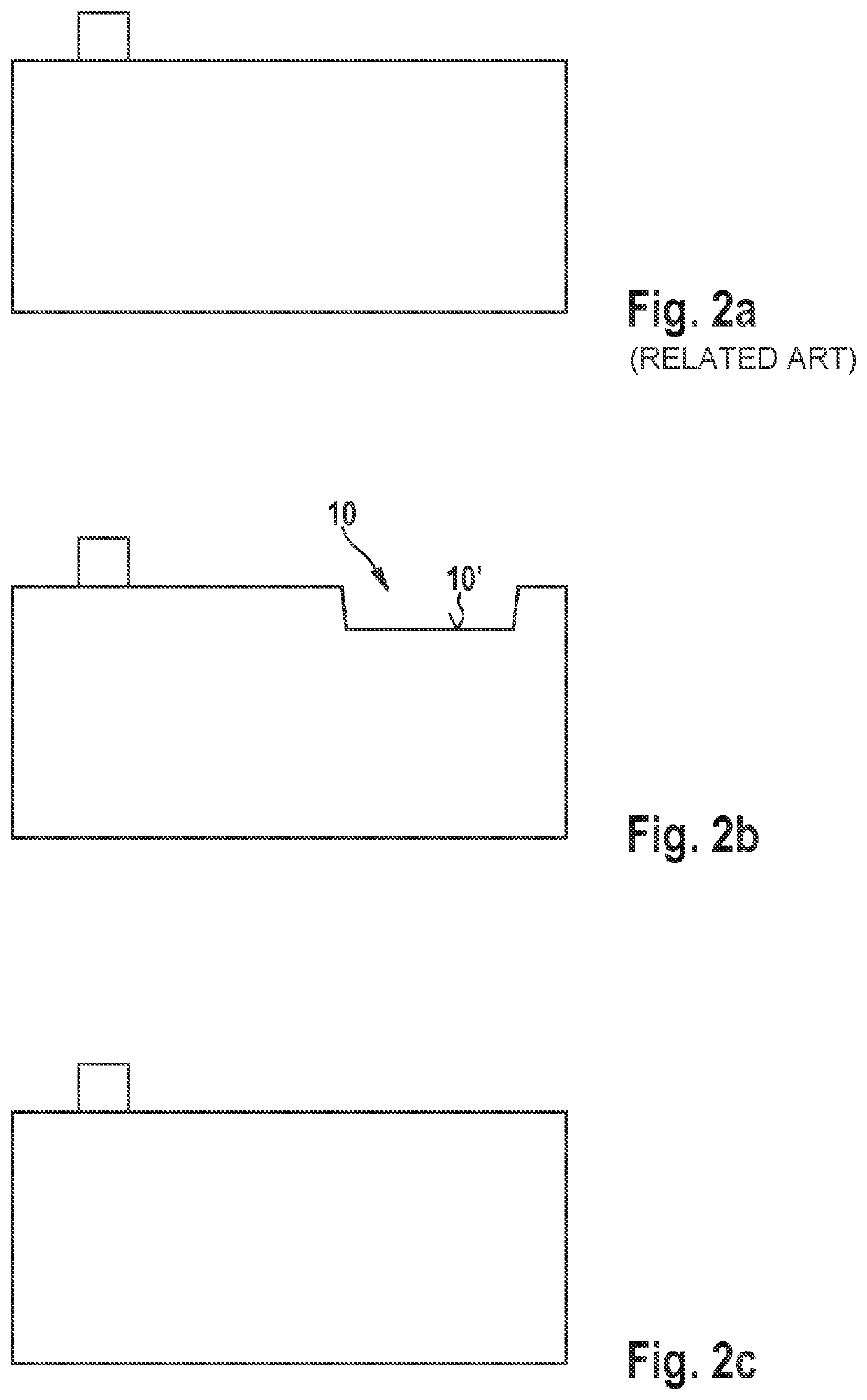
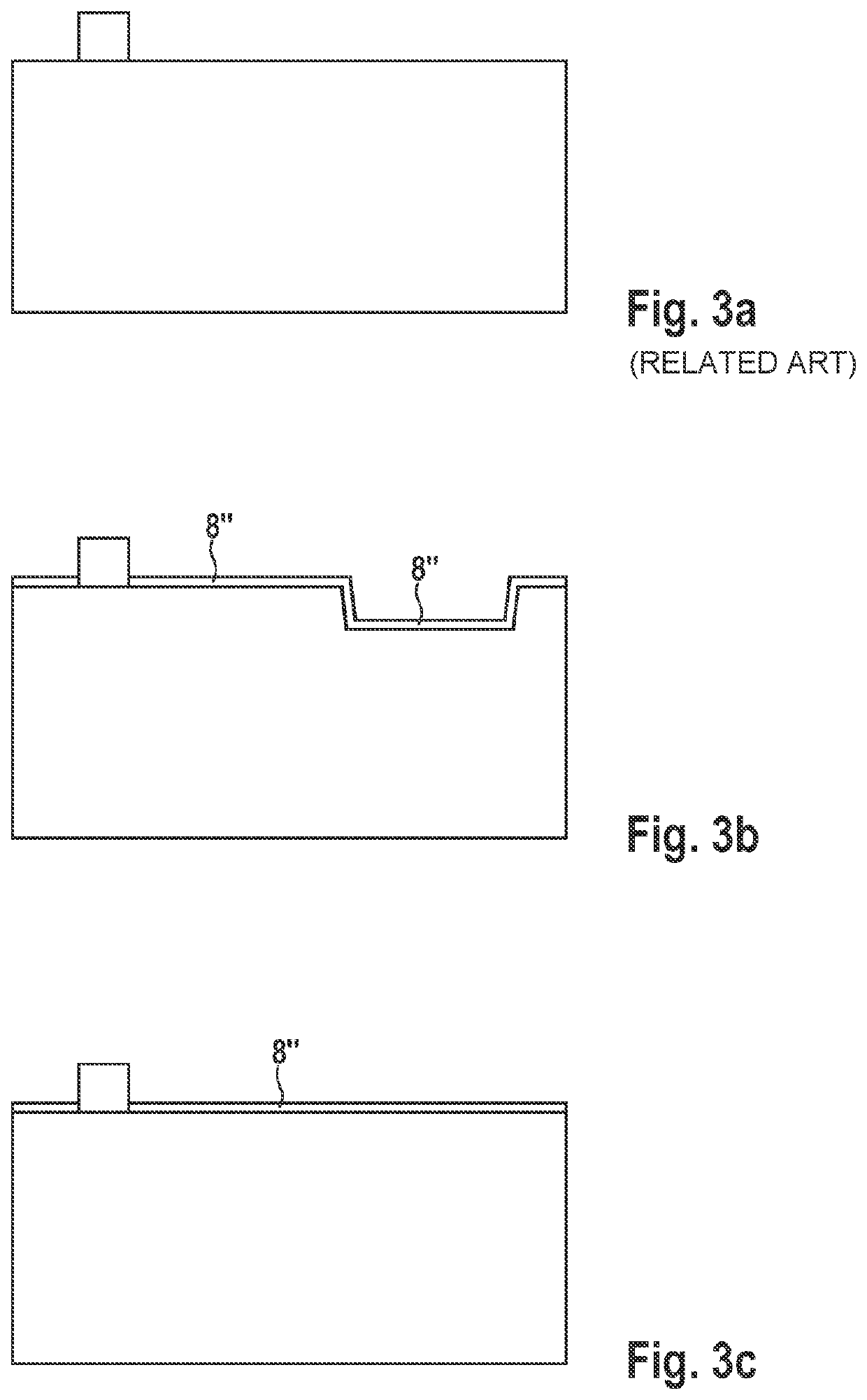
[0026]In the figures, FIGS. 1c, 2c, 3c, 4c, 5c, 6c, 7c, 8c, and 9c correspond to various stages in the production process of a cap wafer 2, or of the sensor 1 formed thereby, according to a specific embodiment of the method according to the present invention. FIGS. 1b, 2b, 3b, 4b, 5b, 6b, 7b, 8b, and 9b show a variant of the method according to the present invention in which, in addition to stop structure 7, a capping electrode 17 is formed as part of cap wafer 2. FIGS. 1a, 2a, 3a, 4a, 5a, 6a, 7a, 8a, and 9a show a production method according to the related art. The respectively corresponding stages of the various production processes are shown one over the other (see for example the sequence of FIGS. 1a, 1b, 1c, which show the respective first substep at the beginning of the processing of the cap wafer), so that the differences, in particular missing or additional substeps, can easily be worked out. In the various Figures, identical or equivalent parts are always provided with the ...


PUM

PropertyMeasurementUnit
thicknessaaaaaaaaaa
thicknessaaaaaaaaaa
heightaaaaaaaaaa

Abstract

A method for producing a microelectromechanical sensor. The microelectromechanical sensor is produced by connecting a cap wafer to a sensor wafer. The cap wafer has a bonding structure for connecting the cap wafer to the sensor wafer. The sensor wafer has a sensor core having a movable structure. The cap wafer has a stop structure for limiting an excursion of the movable structure. The method includes a first step and a second step following the first step, the stop surface of the stop structure being situated at the level of the original surface of the unprocessed cap wafer.

Description

FIELD[0001]The present invention relates to a method for producing a microelectromechanical sensor.BACKGROUND INFORMATION[0002]Microelectromechanical sensors, in particular in the form of inertial sensors, are available the related art in many different specific embodiments. The functional principle of such sensors is generally that an external linear acceleration or rotation applied to the sensor causes inertial forces that cause excursions or deflections of a movable structure in the sensor core, via which the acceleration or rotation can be measured. The movable structure can be etched from a single layer or can be constructed from a plurality of layers. In particular, the movable structure can be formed by epitaxially depositing a silicon layer on a layer made of functional polysilicon (FP), and, in a following step, preparing from the silicon layer a plurality of substructures that are connected to one another via a bridge, formed from the FP layer, of functional polysilicon (F...

Claims


Application Information

Patent Timeline
Patent Type & Authority Applications(United States)
IPC IPC(8): B81C1/00B81B7/00
CPCB81C1/00801B81B7/0025B81C2203/0109B81C2201/014B81B2203/0109B81B3/0051B81B7/0058B81C2203/019G01P15/0802B81C3/001B81C1/00134
Inventor KRONENBERGER, ACHIM
Owner ROBERT BOSCH GMBH
Learn More