Scanning antenna and method for manufacturing scanning antenna
- Summary
- Abstract
- Description
- Claims
- Application Information
AI Technical Summary
Benefits of technology
Problems solved by technology
Method used
Image

Examples
first embodiment
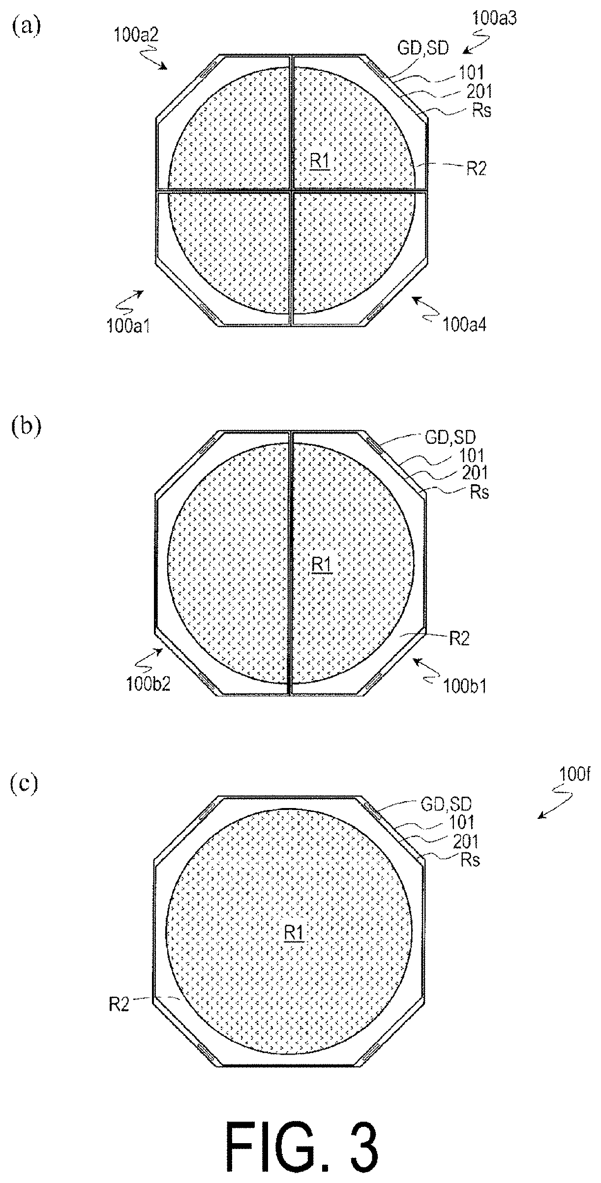
[0121]FIG. 6 is a schematic plan view of one liquid crystal panel 100Aa for preparing a liquid crystal panel of the scanning antenna according to the disclosure by tiling four liquid crystal panels. FIGS. 7(a) to 7(c) are schematic cross-sectional views of the liquid crystal panel 100Aa. FIG. 7(a) illustrates a state immediately after the liquid crystal layer LC is formed (at a room temperature (for example, 25° C.)). FIG. 7(b) illustrates a state in which the volume of liquid crystal material increases (for example, due to increase in the temperature) from the state in FIG. 7(a), and FIG. 7(c) illustrates a state in which the volume of liquid crystal material decreases (for example, due to decrease in the temperature) from the state in FIG. 7(a). Common reference numerals may be assigned to the configuration common to the scanning antenna 1000, and descriptions thereof may be omitted. In the following, an example is described in which the scanning antenna divided into four is prepa...
second embodiment
[0212]Referring to FIG. 15, a structure and manufacturing method of a TFT substrate 101B included in the scanning antenna according to the disclosure. FIGS. 15(a) to 15(e) are schematic cross-sectional views for illustrating the method for manufacturing the TFT substrate 101B, and FIG. 15(f) is a schematic cross-sectional view illustrating the TFT substrate 101B. The following mainly describes differences from the previous embodiment. The constitutions common to the embodiment described above are denoted by the same reference signs and the descriptions thereof may be omitted. The same applies to subsequent embodiments.
[0213]As illustrated in FIG. 15(f), the TFT substrate 101B is different from the previous embodiment in that a contact layer is not provided between the semiconductor layer 5 and the source electrode 7S / drain electrode 7D. As the semiconductor layer 5 of the TFT substrate 101B included in the TFT 10B, an oxide semiconductor layer is used, for example. In the scanning a...
third embodiment
[0225]Referring to FIG. 16, a structure and manufacturing method of a TFT substrate 101C included in the scanning antenna according to the present embodiment. FIGS. 16(a) to 16(e) are schematic cross-sectional views for illustrating the method for manufacturing the TFT substrate 101C, and FIG. 16(f) is a schematic cross-sectional view illustrating the TFT substrate 101C.
[0226]As illustrated in FIG. 16(f), the TFT substrate 101C differs from the TFT substrate 101B in that the TFT substrate 101C further includes a flattened layer 14 between the first insulating layer 11 and the patch metal layer 151. In the scanning antenna including the TFT substrate 101C having such a structure also, the same effect as in the first embodiment can be obtained. The TFT substrate 101C can be applied to any of the liquid crystal panels described above.
[0227]A description is given of a manufacturing method of the TFT substrate 101C with reference to FIGS. 16(a) to 16(e). The description mainly describes ...
PUM
 Abstract
Description
Claims
Application Information