Method for forming a semiconductor device

Pending Publication Date: 2022-03-03
UNITED SEMICONDUCTOR (XIAMEN) CO LTD
View PDF2 Cites 0 Cited by
  • Summary
  • Abstract
  • Description
  • Claims
  • Application Information

AI Technical Summary

Benefits of technology

[0005]It is one object of the present invention to provide an improved semiconductor manufacturing pr

Problems solved by technology

However, the above-mentioned SMT process and self-aligned metal silicide process r

Method used


Image

  • Method for forming a semiconductor device
  • Method for forming a semiconductor device
  • Method for forming a semiconductor device

Examples


Example

[0024]In the following detailed description of the disclosure, reference is made to the accompanying drawings, which form a part hereof, and in which is shown, by way of illustration, specific embodiments in which the invention may be practiced. These embodiments are described in sufficient detail to enable those skilled in the art to practice the invention.

[0025]Other embodiments may be utilized and structural, logical, and electrical changes may be made without departing from the scope of the present invention. Therefore, the following detailed description is not to be considered as limiting, but the embodiments included herein are defined by the scope of the accompanying claims.

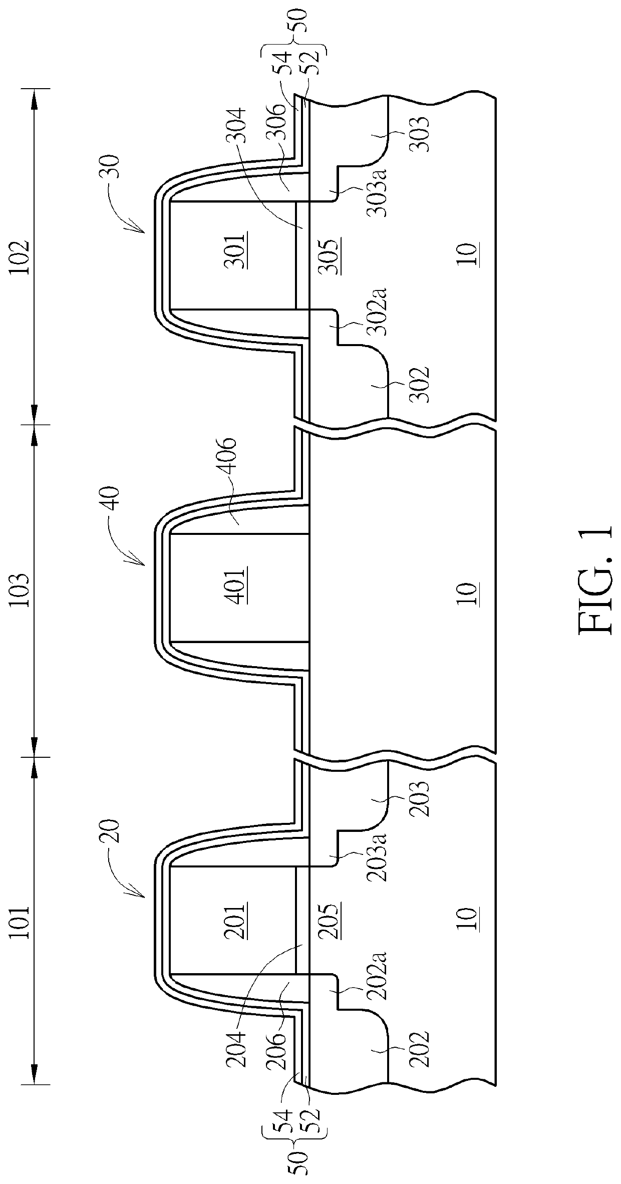
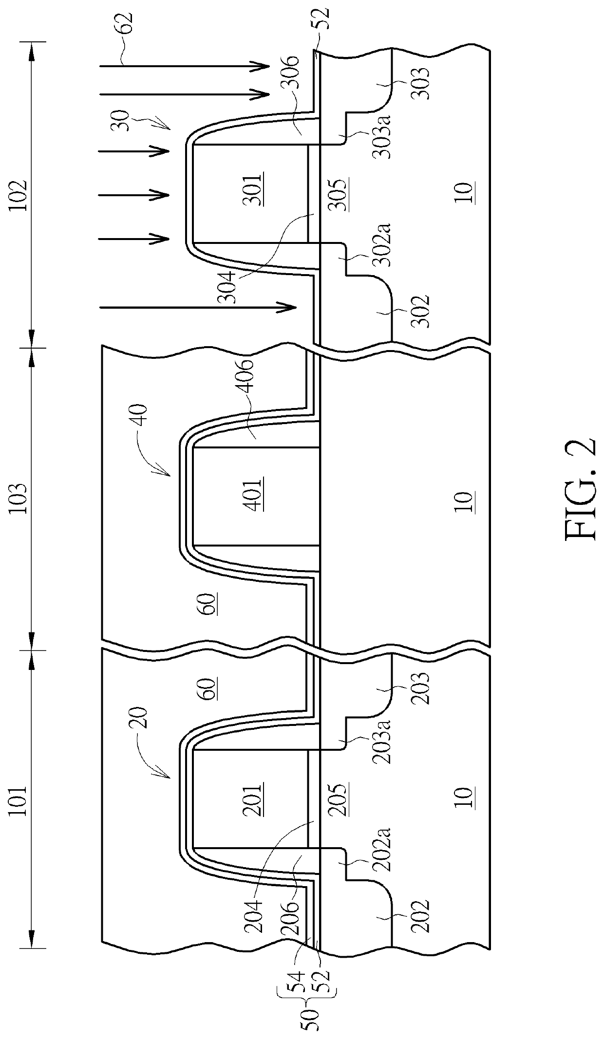
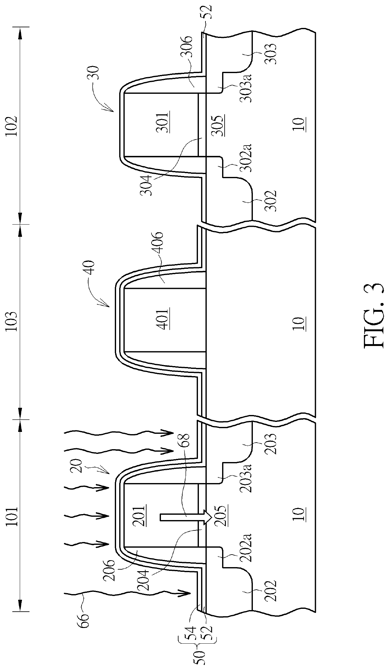
[0026]Please refer to FIGS. 1 to 6, which are schematic cross-sectional views of a method of manufacturing a semiconductor device according to an embodiment of the present invention. As shown in FIG. 1, first, a semiconductor substrate 10, such as a silicon substrate, is provided, but it is not limited the...


PUM


Abstract

A method for forming a semiconductor device is disclosed. A semiconductor substrate having thereon an NMOS region, a PMOS region, and a non-silicide region is provided. An NMOS transistor is formed within the NMOS region and a PMOS transistor is formed within the PMOS region. A stress memorization technique (SMT) layer covering the NMOS region, the PMOS region, and the non-silicide region is formed. The SMT layer is removed from the PMOS region. A stress is transferred from the SMT layer into an N-channel of the NMOS transistor. The SMT layer is removed from the NMOS region, while leaving the SMT layer in the non-silicide region intact. A self-aligned silicidation (SAC) process is performed to form a salicide layer in the NMOS region and the PMOS region.

Description

BACKGROUND OF THE INVENTION1. Field of the Invention[0001]The present invention relates generally to the field of semiconductor manufacturing technology, and particularly relates to a method of manufacturing a semiconductor device.2. Description of the Prior Art[0002]It is known that Stress Memorization Technology (SMT) is usually performed after the source / drain (S / D) ion implantation step in the semiconductor process to induce stress on the channel area of a metal-oxide-semiconductor field effect transistor (MOSFET).[0003]In the conventional SMT process, a stress layer and laser annealing are usually used to induce stress in the substrate, that is, the polysilicon gate under the stress layer is recrystallized by laser annealing to improve the electrical properties of the N-channel MOSFET (NMOSFET, hereinafter referred to as NMOS). The aforementioned stress layer is removed before the subsequent self-aligned silicidation process.[0004]During the self-aligned metal silicide process,...

Claims


Application Information

Patent Timeline
IPC IPC(8): H01L21/8238H01L29/66
CPCH01L21/823807H01L29/7847H01L29/665H01L21/823814H01L21/823821H01L29/6653H01L21/823835
Inventor HU, TAOSHI, XIAO DONGOUYANG, JINJIANTAN, WEN YI
Owner UNITED SEMICONDUCTOR (XIAMEN) CO LTD
Why Eureka
Try Eureka