Broadband Electro-Absorption Optical Modulator Using On-Chip RF Input Signal Termination

a technology of rf input signal and optical modulator, which is applied in the field of electro-absorption optical modulators, can solve the problems of reducing the signal integrity of the system and errors in the modulated output signal, and achieve the effect of maximizing the modulation bandwidth and signal integrity, reducing the transmitter footprint, and being more economical

Pending Publication Date: 2022-03-17
II VI DELAWARE INC
View PDF8 Cites 0 Cited by
  • Summary
  • Abstract
  • Description
  • Claims
  • Application Information

AI Technical Summary

Benefits of technology

[0004]Various advancements over the state of the part are provided by the present invention, which is directed to a broadband EAM that is configured to address these concerns by terminating the high frequency drive signal line within the chip upon which the EAM structure is fabricated. In particular, an AC ground plane is disposed within the EAM structure and separated from the conventional DC ground of the chip substrate by a relatively thin dielectric layer. The combination of the AC ground plane, dielectric layer, and DC ground thus forms a distributed capacitance within the EAM structure that is free of the various parasitics associated with prior art EAM devices. Additional circuit elements, both on-chip and off-chip as described in detail herein, function together to collectively maximize the modulation bandwidth and signal integrity over an extended bandwidth from low modulation frequencies (e.g., 1 GHz or less) up to, and in excess of, 50 GBd / s, while enabling the use of a more economical and compact transmitter footprint than possible for prior art devices.

Problems solved by technology

As optical communication systems continue to be required to transmit data at higher and higher data rates (e.g., in excess of 50 Gbd and above), the high-frequency response of the EAM is a particular area of concern, since limitations in response result in the introduction of errors to the modulated output signal (that is, diminish the signal integrity of the system).

Method used


Image

  • Broadband Electro-Absorption Optical Modulator Using On-Chip RF Input Signal Termination
  • Broadband Electro-Absorption Optical Modulator Using On-Chip RF Input Signal Termination
  • Broadband Electro-Absorption Optical Modulator Using On-Chip RF Input Signal Termination

Examples


Embodiment Construction

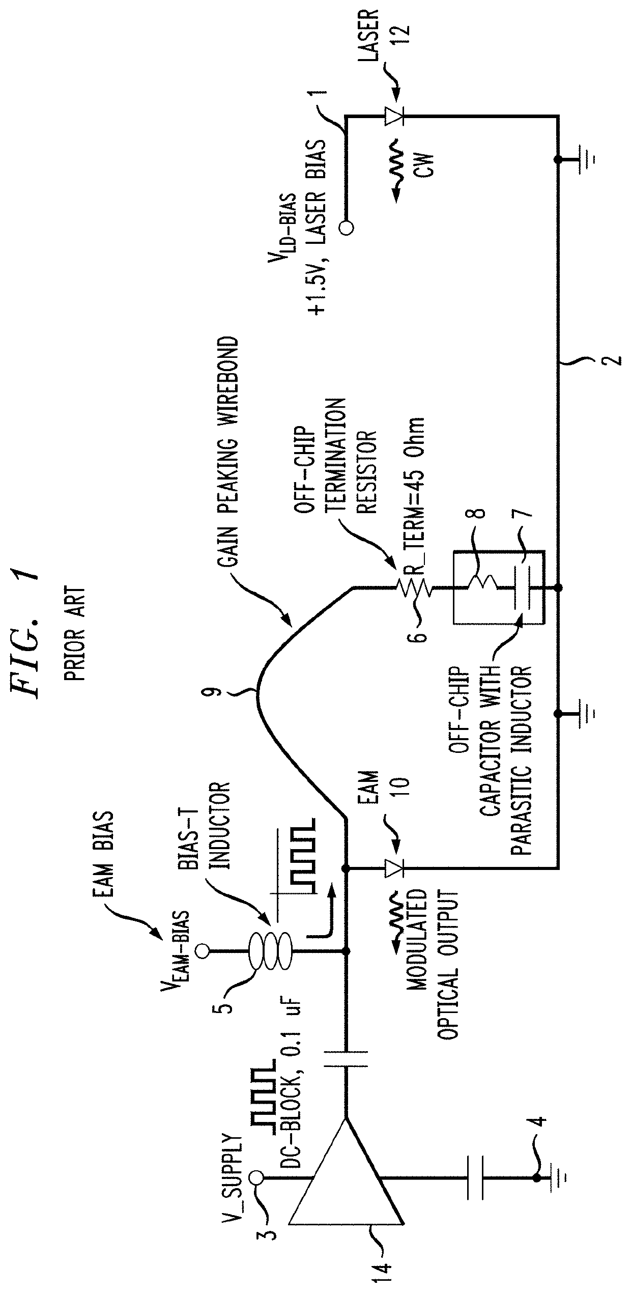
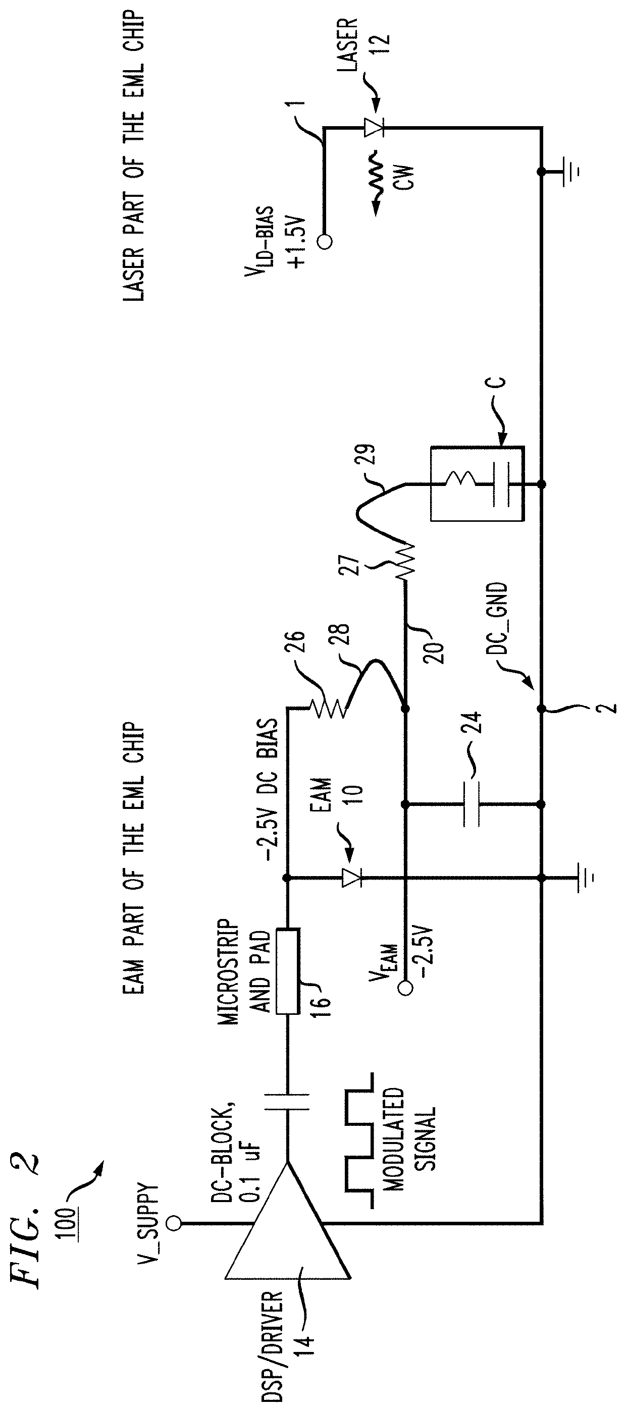
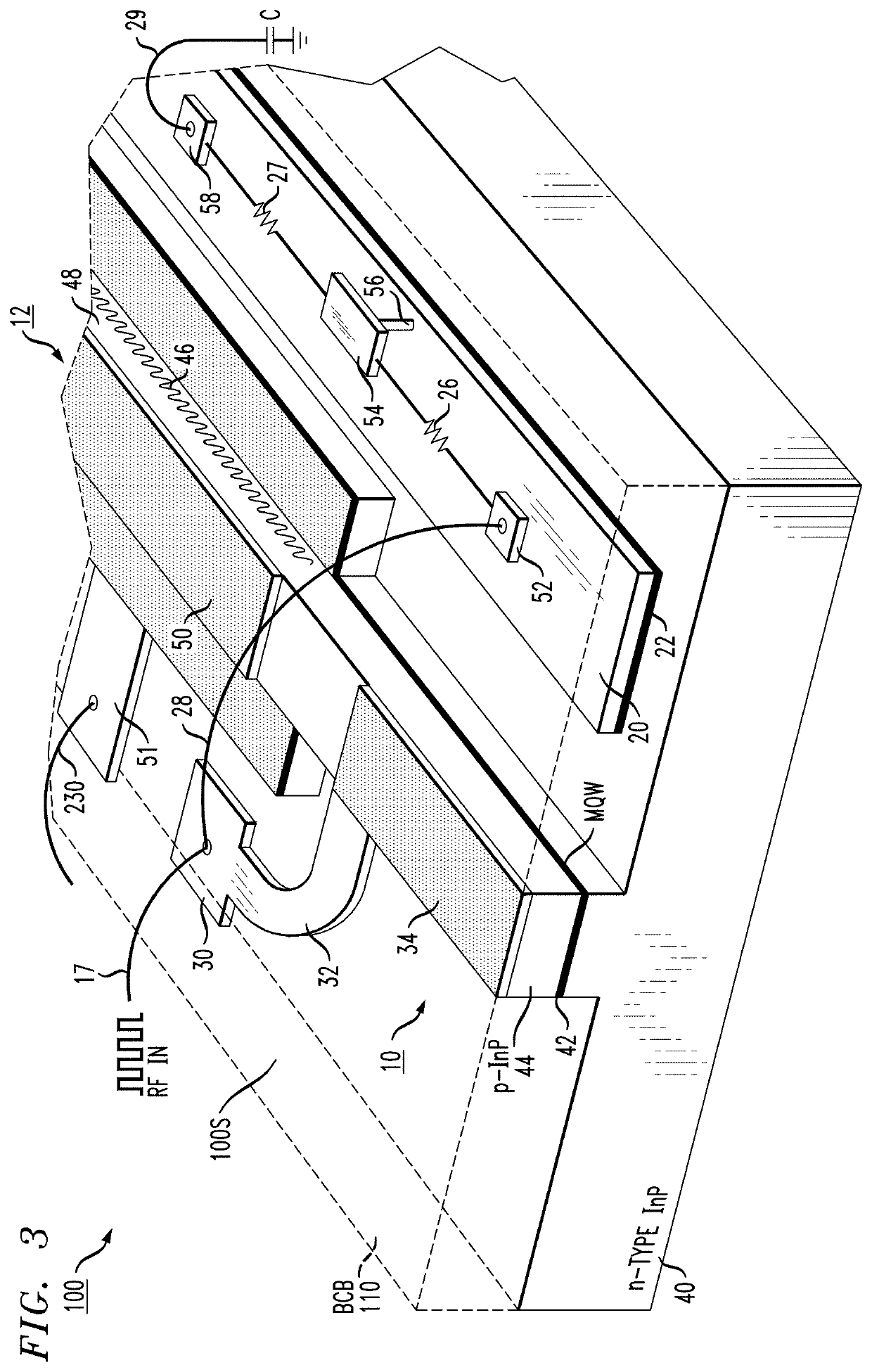
[0017]As mentioned above, optical communication systems continue to be required to transmit data at higher and higher data rates (e.g., in excess of 50 GBd and above) and, as a result, the high-frequency response of an EAM is a particular area of concern, since limitations in its frequency response may result in the introduction of errors in the output modulated optical signal and thus diminish the signal integrity of the system. For EAMs, “signal integrity” typically refers to the fidelity of the output modulated optical waveform when compared to the ideal intended waveform. To optimize the fidelity of the electrical-to-optical conversion between the applied electrical RF drive (data) signal and the output modulated optical signal, there are several performance characteristics that are typically analyzed to assess the operation of the EAM. An exemplary set of performance characteristics may include, for example: (1) the “flatness” of the modulation response over a very large range ...


PUM

PropertyMeasurementUnit
modulation frequenciesaaaaaaaaaa
frequencyaaaaaaaaaa
frequenciesaaaaaaaaaa

Abstract

An electro-absorption modulator (EAM) is configured to include an on-chip AC ground plane that is used to terminate the high frequency RF input signal within the chip itself. This on-chip ground termination of the modulation input signal improves the frequency response of the EAM, which is an important feature when the EAM needs to support data rates in excess of 50 Gbd. By virtue of using an on-chip ground for the very high frequency signal content, it is possible to use less expensive off-chip components to address the lower frequency range of the data signal (i.e., for frequencies less than about 1 GHz).

Description

TECHNICAL FIELD[0001]The present invention relates to electro-absorption optical modulators (EAMs) and, more particularly, to EAMs configured to provide on-chip termination of the applied RF drive signal (electrical data input to EAM).BACKGROUND OF THE INVENTION[0002]Electro-absorption modulators are used in conjunction with laser sources to form an optical transmission arrangement that is relatively compact and based upon the use of relatively low drive voltage levels. In operation, a continuous wave (CW) optical beam from a laser source propagates through a waveguiding region of the EAM, where electrical contacts are positioned above and below the waveguiding region. The application of an electrical data signal to these contacts introduces a change in the optical properties of the waveguide as a function of the change in voltage across the waveguide (as a result of the Franz-Keldysh effect for bulk waveguide structures or the quantum-confined Stark effect for MQW waveguide structu...

Claims


Application Information

Patent Timeline
Patent Type & Authority Applications(United States)
IPC IPC(8): G02F1/025H01S5/06
CPCG02F1/025G02F2001/0157G02F2202/102H01S5/0601H01S5/0265H01S5/0239H01S2301/176H01S5/22H01S5/04257H01S5/12H01S5/34306H01S5/02345H01S5/06226H01S5/0427G02F2202/108G02F2202/101G02F1/0157
Inventor KAIKKONEN, ANDREIADAMS, DAVIDLEWEN, ROBERTCHITICA, NICOLAE
Owner II VI DELAWARE INC
Why Eureka
Try Eureka