Memory device having error detection function, semiconductor device, and electronic device

Pending Publication Date: 2022-03-17
SEMICON ENERGY LAB CO LTD
View PDF0 Cites 0 Cited by
  • Summary
  • Abstract
  • Description
  • Claims
  • Application Information

AI Technical Summary

Benefits of technology

[0027]According to one embodiment of the present invention, a memory device having an error detection function can be provided. Alternatively, according to one embodiment of the present invention, a memory device having an error detection function and enabling a large amount of data to be stored per unit area can be provided.
[0028]Note that the description of these effects does

Problems solved by technology

In the memory device such as a DRAM, an error (mistake) occurs in data stored in the memory cell in

Method used


Image

  • Memory device having error detection function, semiconductor device, and electronic device
  • Memory device having error detection function, semiconductor device, and electronic device
  • Memory device having error detection function, semiconductor device, and electronic device

Examples


embodiment 1

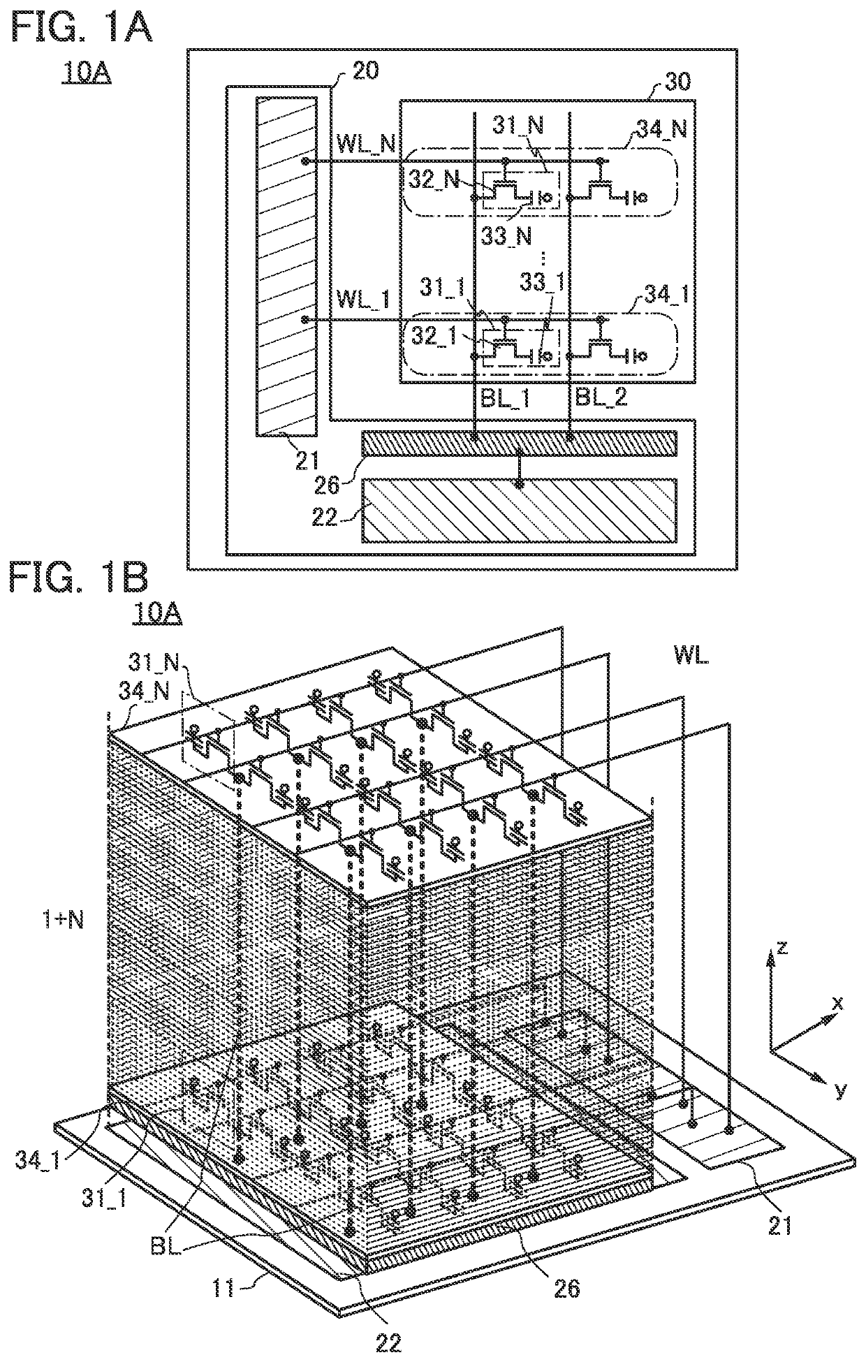
[0074]Structure examples of memory devices of one embodiment of the present invention will be described with reference to FIG. 1 to FIG. 11. The memory devices of one embodiment of the present invention are each a memory device that can function by utilizing semiconductor characteristics, and is also called a memory.

[0075]The memory devices of one embodiment of the present invention each have a structure in which a plurality of layers including OS transistors are stacked over a layer including a transistor formed using a semiconductor substrate. The OS transistor has a characteristic of an extremely low off-state current.

[0076]FIG. 1A is a block diagram illustrating a structure example of a memory device 10A that is one embodiment of the present invention. Note that in the drawings described in this specification and the like, the flow of main signals is indicated by an arrow or a line, and a power supply line and the like are omitted in some cases.

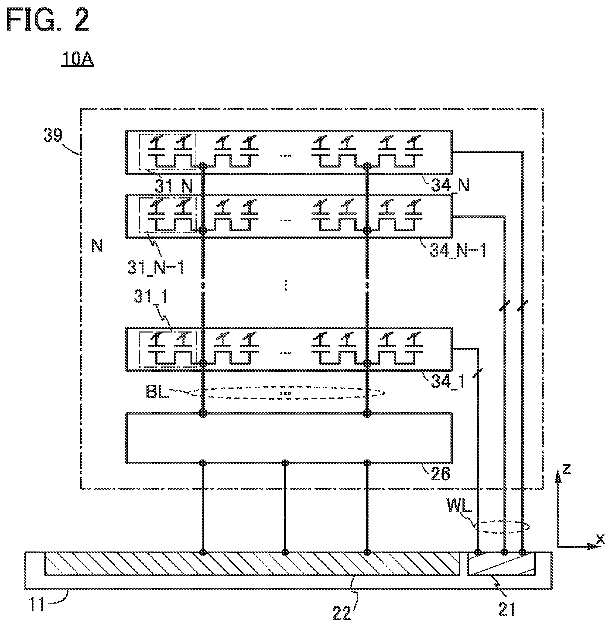
[0077]The memory device 10A includ...

embodiment 2

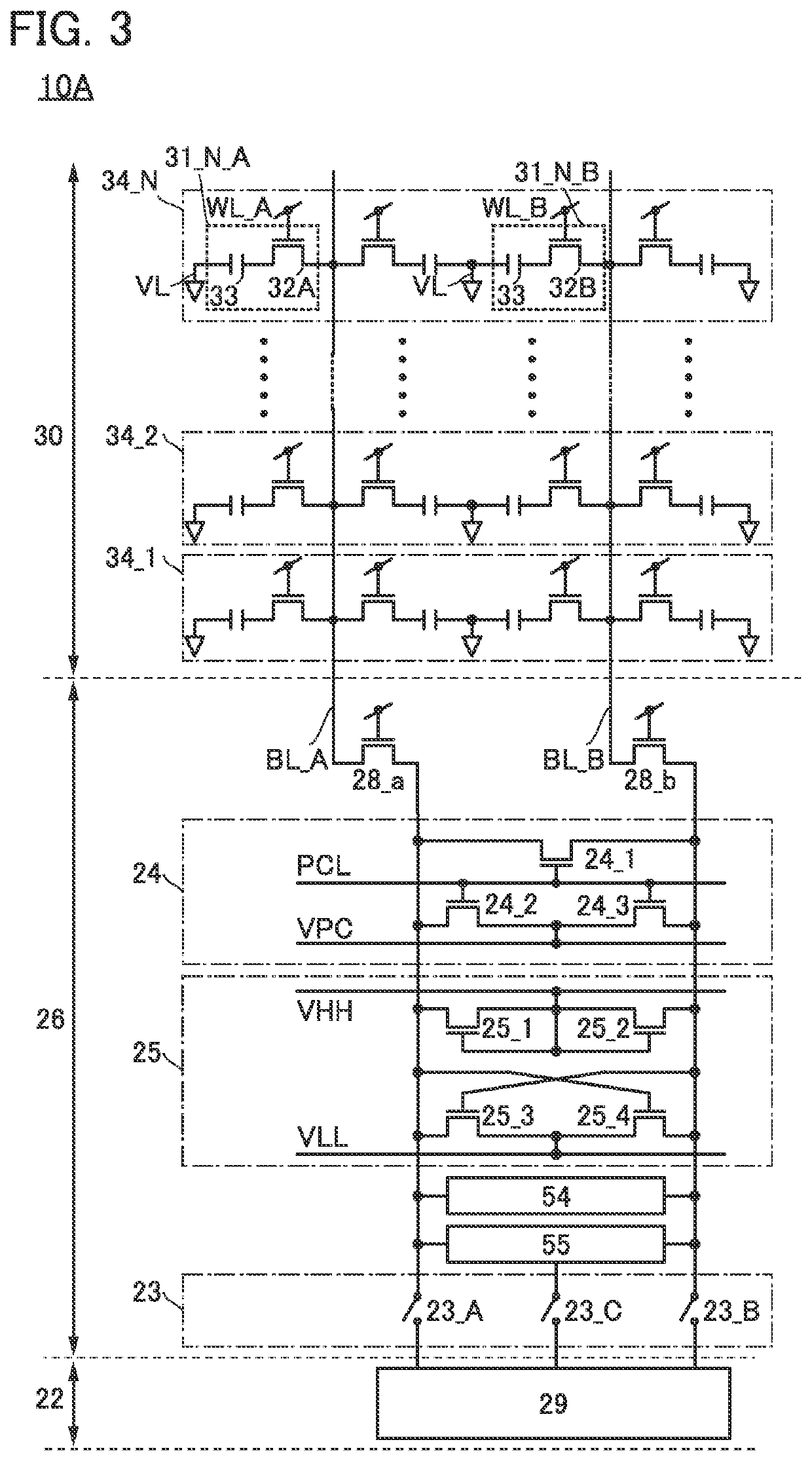
[0145]In this embodiment, a modification example of a circuit applicable to the memory device 10A described in Embodiment 1 will be described with reference to FIG. 12.

[0146]In FIG. 2 and the like, the transistor with a top gate structure or a bottom gate structure without a back gate electrode is shown as the transistors included in the memory cell 31_1 to the memory cell 31_N and the element layer 26. For example, as in a memory device 10C illustrated in FIG. 12, a transistor with a back gate electrode connected to a back gate electrode line BGL may be used. With the structure illustrated in FIG. 12, the threshold voltage of the transistor can be controlled from the outside.

[0147]Note that this embodiment can be implemented in combination with the other embodiments described in this specification as appropriate.

embodiment 3

[0148]An example of a memory device of one embodiment of the present invention will be described below.

[0149]FIG. 13 illustrates an example of a memory device in which memory units 470 (a memory unit 470_1 to a memory unit 470_m: m is a natural number greater than or equal to 1) are stacked over an element layer 411 including a circuit provided using a semiconductor substrate 311. FIG. 13 shows an example in which the element layer 411 and a plurality of memory units 470 over the element layer 411 are stacked, and each of the memory units 470 is provided with one transistor layer 413 (any one of a transistor layer 413_1 to a transistor layer 413_m) and a plurality of memory device layers 415 (a memory device layer 415_1 to a memory device layer 415n: n is a natural number greater than or equal to 2) over the transistor layer 413. Although the example in which the memory device layers 415 are provided over the transistor layer 413 in each of the memory units 470 is shown, this embodi...


PUM


Abstract

A memory device having an error detection function and being capable of storing a large amount of data per unit area is provided. A driver circuit of the memory device is formed using a transistor formed on a semiconductor substrate, and a memory cell of the memory device is formed using a thin film transistor. A plurality of layers each of which includes a memory cell using the thin film transistor can be stacked over the semiconductor substrate, so that the amount of data that can be stored per unit area can be increased. Part of a peripheral circuit including the memory device can be formed using a thin film transistor, and thus, an error detection circuit is formed using the thin film transistor and stacked over the semiconductor substrate.

Description

TECHNICAL FIELD[0001]One embodiment of the present invention relates to a memory device. In particular, one embodiment of the present invention relates to a memory device that can function by utilizing semiconductor characteristics.[0002]One embodiment of the present invention relates to a semiconductor device. In this specification and the like, a semiconductor device refers to a device that utilizes semiconductor characteristics and indicates, for example, a circuit including a semiconductor element (a transistor, a diode, a photodiode, and the like), a device including the circuit, and the like. Note that in this specification and the like, a semiconductor device refers to any device that can function by utilizing semiconductor characteristics; examples of the semiconductor device include an integrated circuit, a chip provided with an integrated circuit, an electronic component in which a chip is incorporated in a package, and an electronic device provided with an integrated circ...

Claims


Application Information

Patent Timeline
IPC IPC(8): H01L27/108H01L21/8239H01L29/786G11C29/52
CPCH01L27/108G11C29/52H01L29/7869H01L21/8239G11C5/025G11C2029/0411G11C29/12015G11C2029/0403G11C11/4097G06F11/1004H01L27/0688H10B12/00H10B41/70H10B99/00
Inventor KUNITAKE, HITOSHIONUKI, TATSUYAATSUMI, TOMOAKIKATO, KIYOSHI
Owner SEMICON ENERGY LAB CO LTD
Why Eureka
Try Eureka