Semiconductor device and method for producing same

a semiconductor chip and semiconductor technology, applied in the direction of semiconductor/solid-state device details, antenna details, antennas, etc., to achieve the effect of suppressing the occurrence of a positional shift of a semiconductor chip during resin sealing and forming easily and accurately

Pending Publication Date: 2022-03-31
NAGASE & COMPANY
View PDF0 Cites 0 Cited by
  • Summary
  • Abstract
  • Description
  • Claims
  • Application Information

AI Technical Summary

Benefits of technology

[0026]With the present invention, the occurrence of a positional shift of a semiconductor chip during resin sealing can be suppressed, and a redistribution layer can be easily and accurately formed.

Problems solved by technology

The semiconductor chip is sealed within an insulating layer by a thermosetting process of the mold resin, which has a problem of an occurrence of a positional shift of the semiconductor chips placed on the wafer due to a shrinkage effect of the resin and a thermal expansion effect of the wafer during the thermosetting process.
In the case of employing a process of resin sealing after the semiconductor chips are disposed on the wafer, a chip surface and a mold surface do not always become flush to possibly cause a level difference therebetween, and thus, there lies a problem that the level difference causes various failures when a redistribution layer is formed on the chip surface.

Method used


Image

  • Semiconductor device and method for producing same
  • Semiconductor device and method for producing same
  • Semiconductor device and method for producing same

Examples


first embodiment

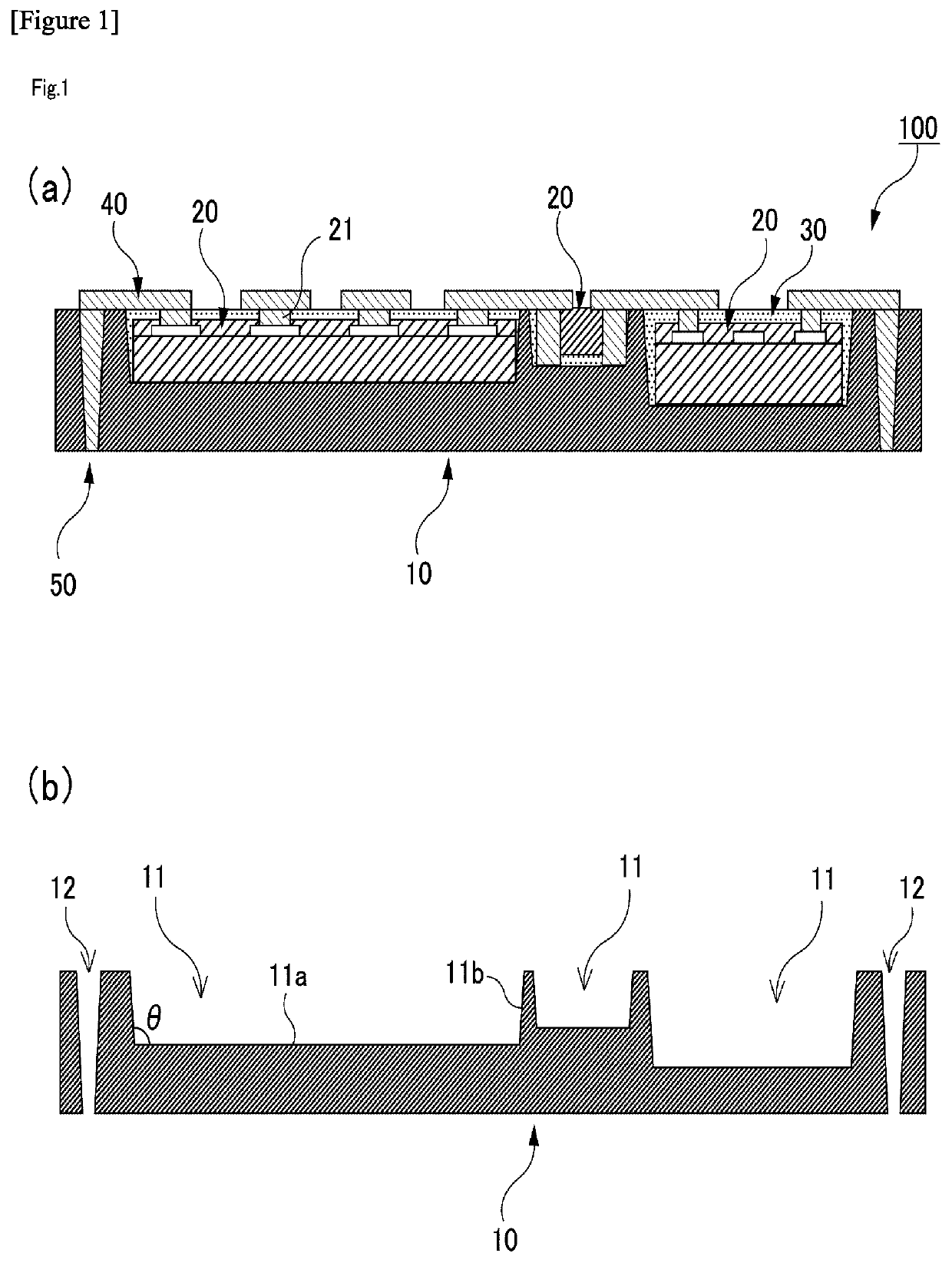
[0039]FIG. 1 is a cross-sectional view of a semiconductor device 100 according to the present invention. As illustrated in FIG. 1, the semiconductor device 100 is a wafer level package configured by including a substrate 10, circuit elements 20, and redistribution layers 40. FIG. 1(a) illustrates a cross-sectional structure of the whole semiconductor device 100, and FIG. 1(b) illustrates a cross-sectional structure of the substrate 10 only.

[0040]The substrate 10 can be obtained by performing a thermosetting process after molding an uncured thermosetting resin into a predetermined shape. Accordingly, the substrate 10 is formed of a cured thermosetting resin. As the thermosetting resin, for example, an epoxy resin, a polyimide resin, a phenol resin, a cyanate resin, a polyester resin, an acrylic resin, a bismaleimide resin, a benzoxazine resin, or a mixed resin of one type or two or more types of these can be used.

[0041]More specifically describing, as the thermosetting resin that for...

second embodiment

[0067]In the second embodiment, insulating films 70 are formed so as to cover the redistribution layers 40 on both surfaces of the substrate 10. The insulating film 70 almost entirely covers the semiconductor device 100 except for a part of openings 71. The opening 71 of the insulating film 70 is disposed so as to expose metallic materials that constitute the redistribution layers 40 on the front surface and / or the back surface of the substrate 10. Accordingly, another semiconductor device or circuit element can be connected to the redistribution layer 40 via the opening 71 of the insulating film 70.

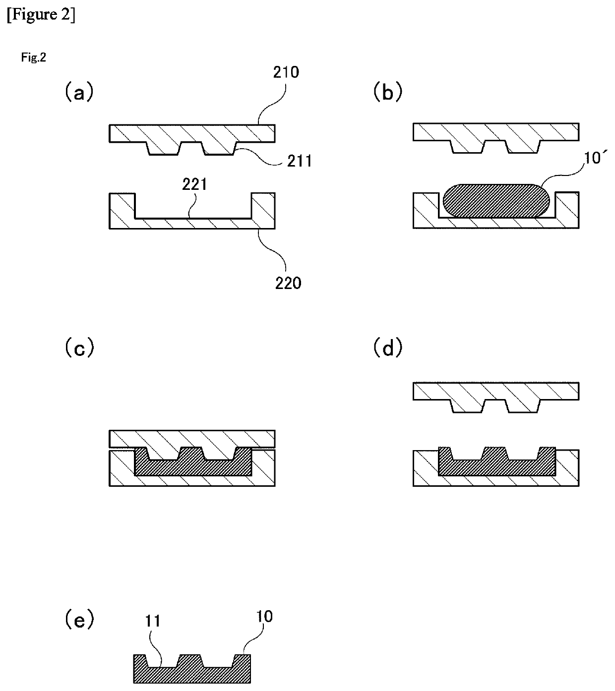
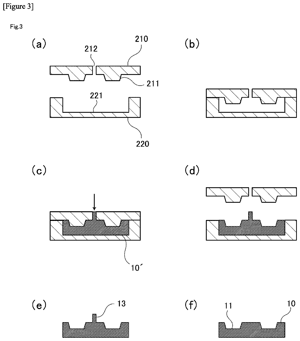
[0068]FIG. 7 illustrates an exemplary production process of the semiconductor device 100 according to the second embodiment. As illustrated in FIG. 7(a), first, the substrate 10 having the front surface and the back surface on which the recesses 11 are formed is prepared. The method for forming the substrate 10 may be performed in compliant with the compression method illustrated in FIG....


PUM

PropertyMeasurementUnit
Tgaaaaaaaaaa
Tgaaaaaaaaaa
decomposition temperatureaaaaaaaaaa

Abstract

The occurrence of a positional shift of a semiconductor chip during resin sealing is suppressed; and a redistribution layer is easily and accurately formed. A semiconductor device according to the present invention is provided with: a substrate which is formed of a cured thermosetting resin, and which has one or more recesses; a circuit element which is arranged within a recess of the substrate; and a redistribution layer which is connected to the circuit element on the opening side of the recess.

Description

TECHNICAL FIELD[0001]The present invention relates to a semiconductor device and a method for producing the same.BACKGROUND ART[0002]When producing a semiconductor device, there has conventionally known a technique that arranges a plurality of diced semiconductor chips on a wafer substrate and seals the semiconductor chips with a thermosetting mold resin (Patent Document 1). The semiconductor chip is sealed within an insulating layer by a thermosetting process of the mold resin, which has a problem of an occurrence of a positional shift of the semiconductor chips placed on the wafer due to a shrinkage effect of the resin and a thermal expansion effect of the wafer during the thermosetting process. In the case of employing a process of resin sealing after the semiconductor chips are disposed on the wafer, a chip surface and a mold surface do not always become flush to possibly cause a level difference therebetween, and thus, there lies a problem that the level difference causes vario...

Claims


Application Information

Patent Timeline
Patent Type & Authority Applications(United States)
IPC IPC(8): H01L23/00H01L23/29H01L23/31H01L23/538H01L23/66H01L21/48H01L21/56
CPCH01L24/20H01L23/291H01L23/3121H01L23/5383H01L23/5386H01L23/5389H01L2224/214H01L24/19H01L21/4853H01L21/4857H01L21/565H01L2223/6677H01L23/66H01L2224/18H01L2924/19105H01Q19/12H01L2924/15153H01L2224/12105H01L2224/04105H01L2224/92244H01L2224/73267H01L2224/97H01L2224/32225H01L2224/24195H01Q1/2283H01L23/13H01L23/145H01L2224/83H01L23/14H01L23/18H01Q1/38H01L21/56
Inventor SATOTAKANO, TADASHI
Owner NAGASE & COMPANY
Why Eureka
Try Eureka