Bitline precharge system for a semiconductor memory device

a memory device and pre-charge technology, applied in the field of memory access systems, can solve the problems of significant power consumption of sram for pre-charging bitlines, dynamic power consumption has not been scaled down to the same extent, etc., and achieve the effects of enhancing reliability, reducing dynamic power consumption, and conserving system power

Active Publication Date: 2022-04-07
SAMSUNG ELECTRONICS CO LTD
View PDF0 Cites 1 Cited by
  • Summary
  • Abstract
  • Description
  • Claims
  • Application Information

AI Technical Summary

Benefits of technology

[0005]Many emerging technologies such as Internet of Things (IOT), cloud computing, servers, networking, and the like contain processers that are in an active mode for most of the processors' lifetimes. Thus, reducing dynamic power consumption may conserve system power as well as enhance reliability.
[0006]Exemplary embodiments of the present disclosure are provided for controlling voltage levels of a bitline (BL) as a function of a wordline (WL) supply level. Specifically, an exemplary embodiment is provided for reducing clock power and an overall dynamic power of an SRAM device, without limitation thereto.

Problems solved by technology

Despite advances in technology including substantially scaled down form factors, dynamic power consumption has not scaled down to the same extent.
The SRAM may consume significant power for pre-charging the bitlines to a VDD level.

Method used


Image

  • Bitline precharge system for a semiconductor memory device
  • Bitline precharge system for a semiconductor memory device
  • Bitline precharge system for a semiconductor memory device

Examples


Embodiment Construction

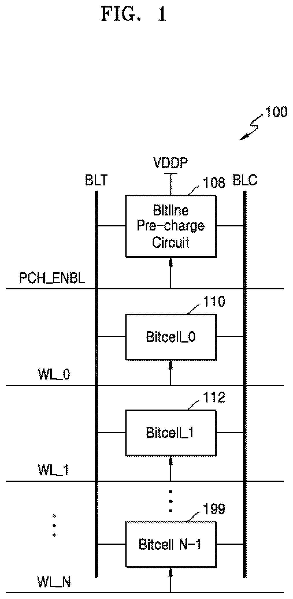
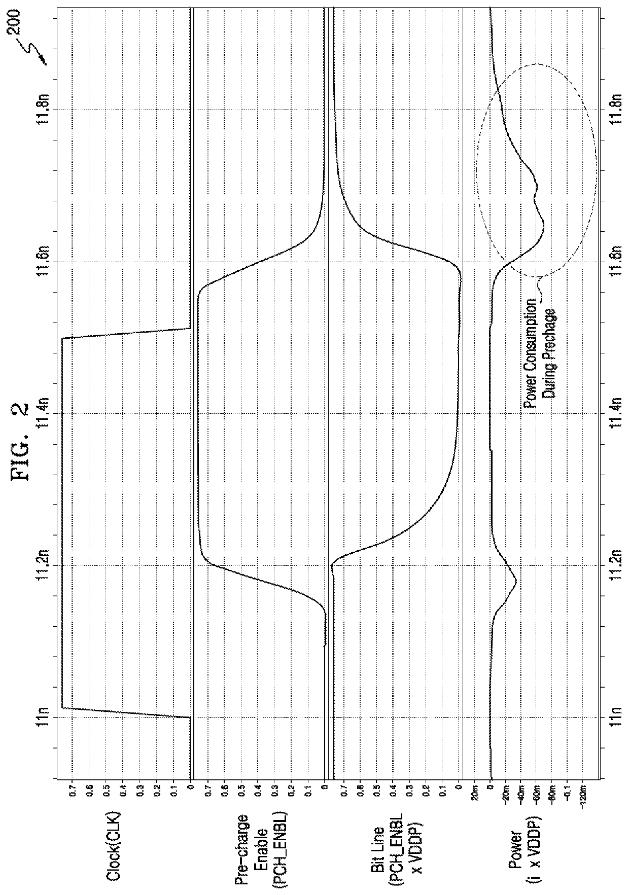
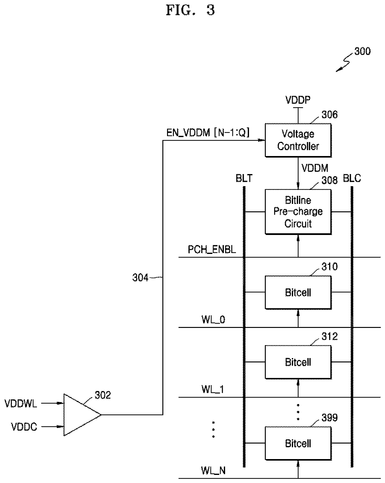
[0019]For the purpose of promoting an understanding of the principles of the disclosure, reference will now be made to the exemplary embodiments illustrated in the drawings and specific language will be used to describe the same. It will nevertheless be understood that no limitation of the scope of the disclosure is thereby intended. For example, alterations and further modifications in the illustrated systems may be applied, and such further applications of the principles of the disclosure as illustrated therein are contemplated as would normally occur to one skilled in the art to which the disclosure relates.

[0020]It will be understood by those skilled in the art that the foregoing general description and the following detailed description are explanatory of the disclosure and are not intended to be restrictive thereof.

[0021]Reference throughout this specification to “an embodiment” or similar language means that a particular feature, structure, or characteristic described in conn...


PUM


Abstract

A bitline precharge system is provided for a semiconductor memory device. The bitline precharge system comprises a voltage comparator circuit to output a reference voltage signal based on an input wordline voltage supply level (VDDWL), and a periphery power supply voltage (VDDP) level. A voltage control circuit is electrically coupled to a periphery power supply and the voltage comparator circuit to output a precharge voltage (VDDM) level based on the reference voltage signal and the periphery power supply voltage (VDDP) level. A bitline precharge circuit is electrically coupled to the voltage control circuit and a plurality of bitlines of the memory device to precharge the plurality of bitlines based on the precharge voltage (VDDM) level in response to a precharge enable signal during one of a read operation to read data from the memory device and a write operation to write data from the memory device. Further, the at least one bitline is discharged from the precharge voltage (VDDM) level during at least one of the read operation or the write operation.

Description

CROSS-REFERENCE[0001]The present application claims priority under 35 U.S.C. § 119 to Indian patent application number 202041042804, filed on Oct. 1, 2020 in the Indian Patent Office, the entire disclosure of which is incorporated by reference.FIELD[0002]The present disclosure generally relates to memory-access systems, and particularly relates to memory-access precharge systems.DISCUSSION OF RELATED ART[0003]Despite advances in technology including substantially scaled down form factors, dynamic power consumption has not scaled down to the same extent. One possible reason may be attributed to the fact that since gate capacitance of fin field-effect transistor (FinFET) devices may be more than planar metal-oxide-semiconductor field-effect transistor (MOSFET) devices, a greater amount of capacitance may have to be charged and / or discharged to achieve like functionality. The scaling of static random-access memory (SRAM) operating voltages may be diminished to very low levels in advanc...

Claims


Application Information

Patent Timeline
Patent Type & Authority Applications(United States)
IPC IPC(8): G11C11/419
CPCG11C11/419G11C7/12
Inventor PULLURU, LAVA KUMARGUPTA, ANKURRANA, PARVINDER KUMAR
Owner SAMSUNG ELECTRONICS CO LTD
Why Eureka
Try Eureka