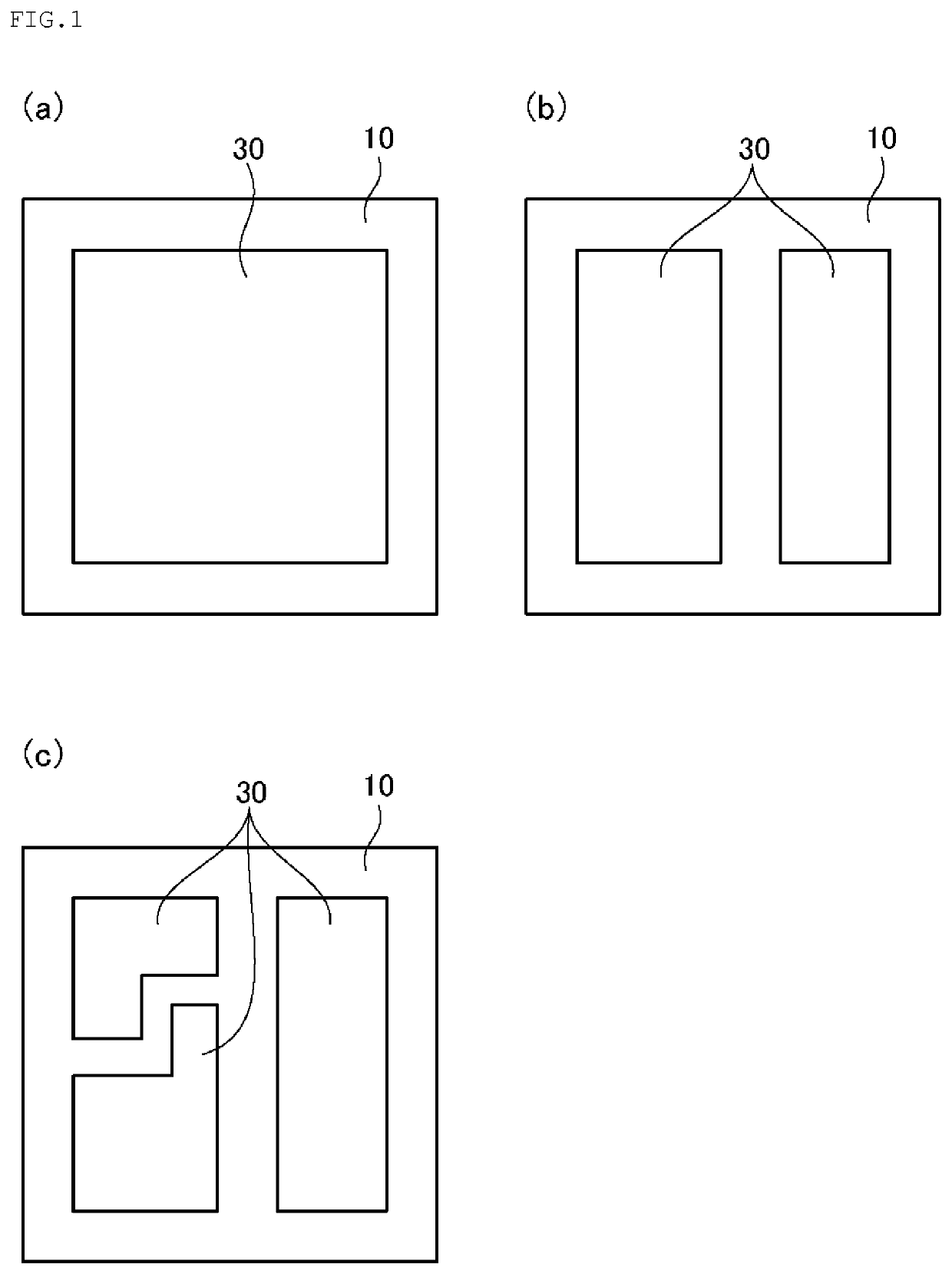
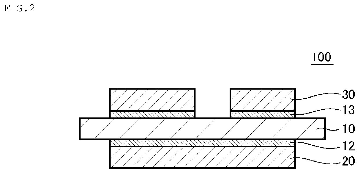
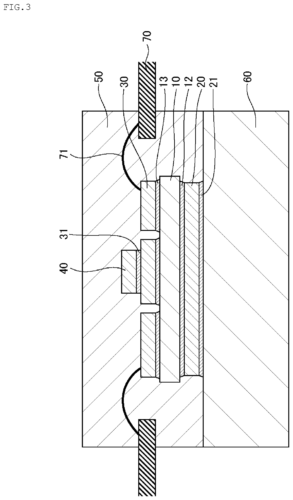
Silicon nitride circuit board and electronic component module
a technology of silicon nitride and electronic components, applied in the direction of basic electric elements, metal pattern materials, solid-state devices, etc., can solve the problems of poor thermal resistance, poor bonding strength, and low operational reliability of electronic devices, and achieve poor thermal resistance, poor bonding strength, and low occurrence rate
- Summary
- Abstract
- Description
- Claims
- Application Information
AI Technical Summary
Benefits of technology
Problems solved by technology
Method used
Image

Examples
examples
[0090]The present invention will be described below in detail with reference to Examples, but the present invention is not limited to the description of these Examples.
[0091]A plurality of silicon nitride circuit boards having different HS1, HS2, and fracture toughness values Kc were prepared by a method as follows, and a heat cycle test described below was performed.
[0092]
[0093]Silicon nitride substrates B-1 to B-10 (148 mm×200 mm×0.32 mm) having various coefficients of linear expansion αB, Young's moduli EB, and fracture toughness values Kc were prepared by adjusting the blending of the raw materials and the baking conditions.
[0094]
[0095]A rolled copper plate of which the coefficient of linear expansion is 17.3×10⁻⁶ / ° C. and a thickness is 0.8 mm was prepared.
[0096]
[0097]Silicon nitride circuit boards 1 to 10 were manufactured by using the silicon nitride substrates and the copper plates of a combinations shown in Table 1.
[0098]First, as the brazing material (including active meta...
PUM
| Property | Measurement | Unit |
|---|---|---|
| fracture toughness | aaaaa | aaaaa |
| fracture toughness | aaaaa | aaaaa |
| average crystal grain size | aaaaa | aaaaa |
Abstract
Description
Claims
Application Information
 - Generate Ideas
- Intellectual Property
- Life Sciences
- Materials
- Tech Scout
- Unparalleled Data Quality
- Higher Quality Content
- 60% Fewer Hallucinations
Browse by: Latest US Patents, China's latest patents, Technical Efficacy Thesaurus, Application Domain, Technology Topic, Popular Technical Reports.
© 2025 PatSnap. All rights reserved.Legal|Privacy policy|Modern Slavery Act Transparency Statement|Sitemap|About US| Contact US: help@patsnap.com