Photoelectric conversion element and imaging device
a conversion element and imaging device technology, applied in the direction of radiation controlled devices, semiconductor devices, semiconductor/solid-state device details, etc., can solve the problems of inability to obtain sufficient external quantum efficiency, easy delay of electric output signal with respect to incident light,
- Summary
- Abstract
- Description
- Claims
- Application Information
AI Technical Summary
Benefits of technology
Problems solved by technology
Method used
Image

Examples
modification example 2 (
2-2. Modification Example 2 (An example of a photoelectric conversion element in which a plurality of organic photoelectric conversion sections is stacked)
3. Application Examples
4. Practical Application Examples
5. Working Examples
1. EMBODIMENT
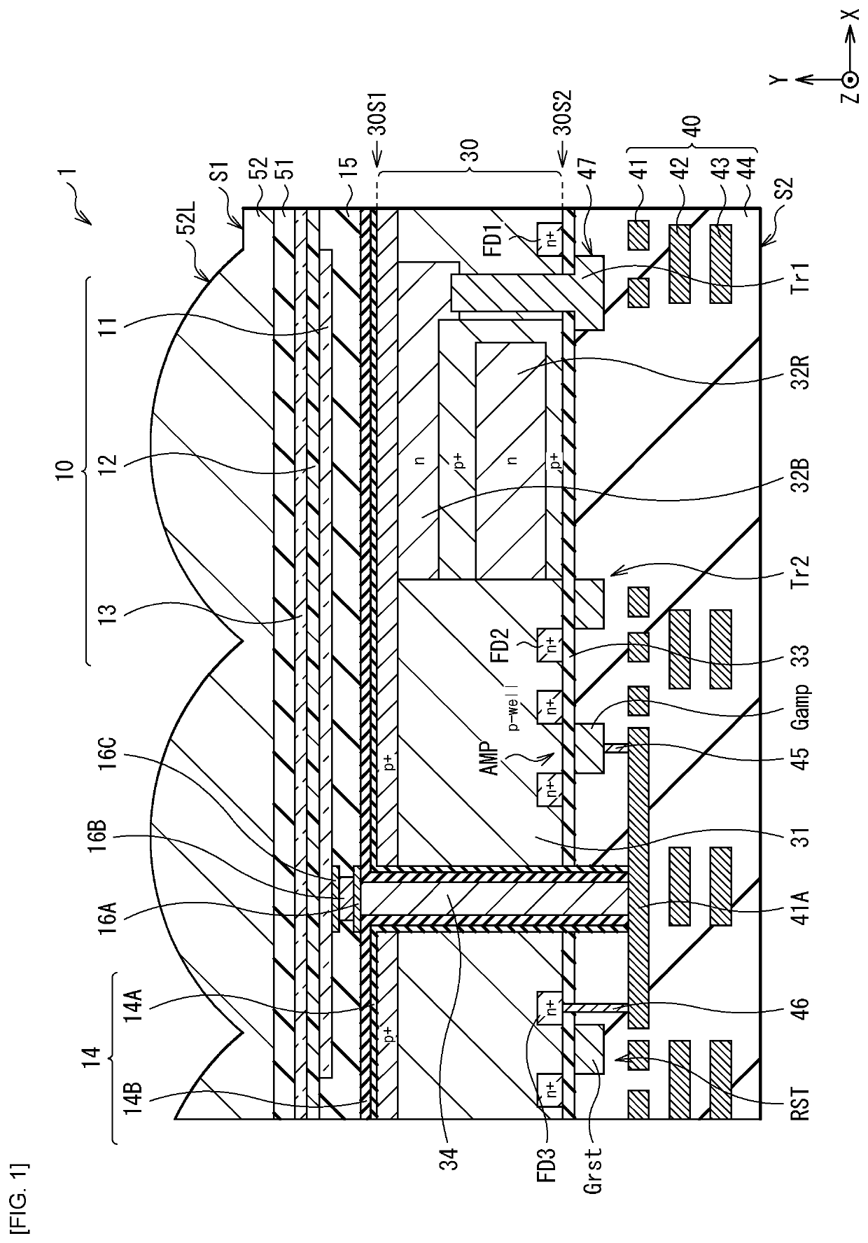
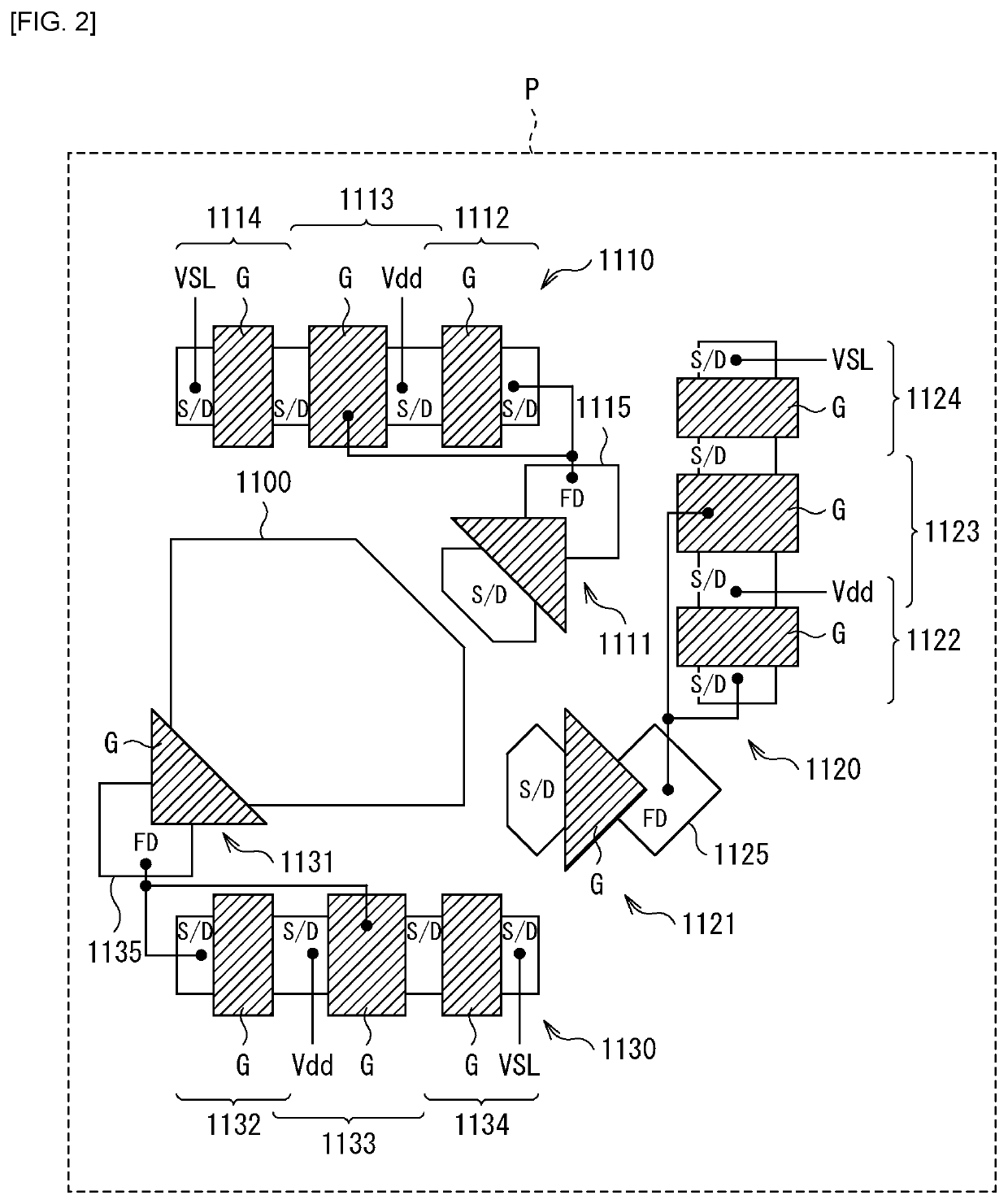
[0043]FIG. 1 illustrates an example of a cross-sectional configuration of a photoelectric conversion element (a photoelectric conversion element 1) according to an embodiment of the present disclosure. FIG. 2 illustrates an example of a planar configuration of the photoelectric conversion element 1 illustrated in FIG. 1. The photoelectric conversion element 1 is included, for example, in one pixel (a unit pixel P) in a solid-state imaging device (an imaging device 100) such as a back-illuminated (back light receiving) CCD (Charge Coupled Device) image sensor or CMOS (Complementary Metal Oxide Semiconductor) image sensor (see FIG. 12). The photoelectric conversion element 1 is of a so-called vertical spectroscopic type in which one organic photo...
modification examples
2. MODIFICATION EXAMPLES
2-1. Modification Example 1
[0129]FIG. 8 illustrates an example of a cross-sectional configuration of an imaging element (a photoelectric conversion element 2) according to a modification example 1 of the present disclosure. FIG. 9 is an equivalent circuit diagram of the photoelectric conversion element 2 illustrated in FIG. 8. FIG. 10 schematically illustrates the disposition of a lower electrode 21 of the photoelectric conversion element 2 illustrated in FIG. 8 and a transistor included in a controller. The photoelectric conversion element 2 is included, for example, in one pixel (the unit pixel P) in the solid-state imaging device (the imaging device 100) such as a back-illuminated (back light receiving) CCD image sensor or CMOS image sensor as in the embodiment described above. Although described in detail below, the lower electrode 21 of the photoelectric conversion element 2 according to the present modification example includes a readout electrode 21A a...
modification example 2
2-2. Modification Example 2
[0161]FIG. 11 illustrates a cross-sectional configuration of a photoelectric conversion element (a photoelectric conversion element 3) according to a modification example 2 of the present disclosure. The photoelectric conversion element 3 is included, for example, in the one unit pixel Pin the solid-state imaging element (the imaging device 100) such as a back-illuminated CCD image sensor or CMOS image sensor as with the photoelectric conversion element 1 according to the embodiment or the like described above. The photoelectric conversion element 3 according to the present modification example has a configuration in which a red photoelectric conversion section 70R, a green photoelectric conversion section 70G, and a blue photoelectric conversion section 70B are stacked in this order on the semiconductor substrate 30 with the insulating layer 76 interposed in between.
[0162]The red photoelectric conversion section 70R, the green photoelectric conversion sec...
PUM
| Property | Measurement | Unit |
|---|---|---|
| wavelength band | aaaaa | aaaaa |
| wavelength band | aaaaa | aaaaa |
| selective wavelength | aaaaa | aaaaa |
Abstract
Description
Claims
Application Information
 - R&D
- Intellectual Property
- Life Sciences
- Materials
- Tech Scout
- Unparalleled Data Quality
- Higher Quality Content
- 60% Fewer Hallucinations
Browse by: Latest US Patents, China's latest patents, Technical Efficacy Thesaurus, Application Domain, Technology Topic, Popular Technical Reports.
© 2025 PatSnap. All rights reserved.Legal|Privacy policy|Modern Slavery Act Transparency Statement|Sitemap|About US| Contact US: help@patsnap.com