

Defect inspection apparatus, method for inspecting defect, and method for manufacturing photomask blank
a technology for defect inspection and inspection apparatus, applied in the direction of originals for photomechanical treatment, semiconductor/solid-state device testing/measurement, instruments, etc., can solve problems such as defect transfer
- Summary
- Abstract
- Description
- Claims
- Application Information
AI Technical Summary
Benefits of technology
Problems solved by technology
Method used
Image

Examples
example
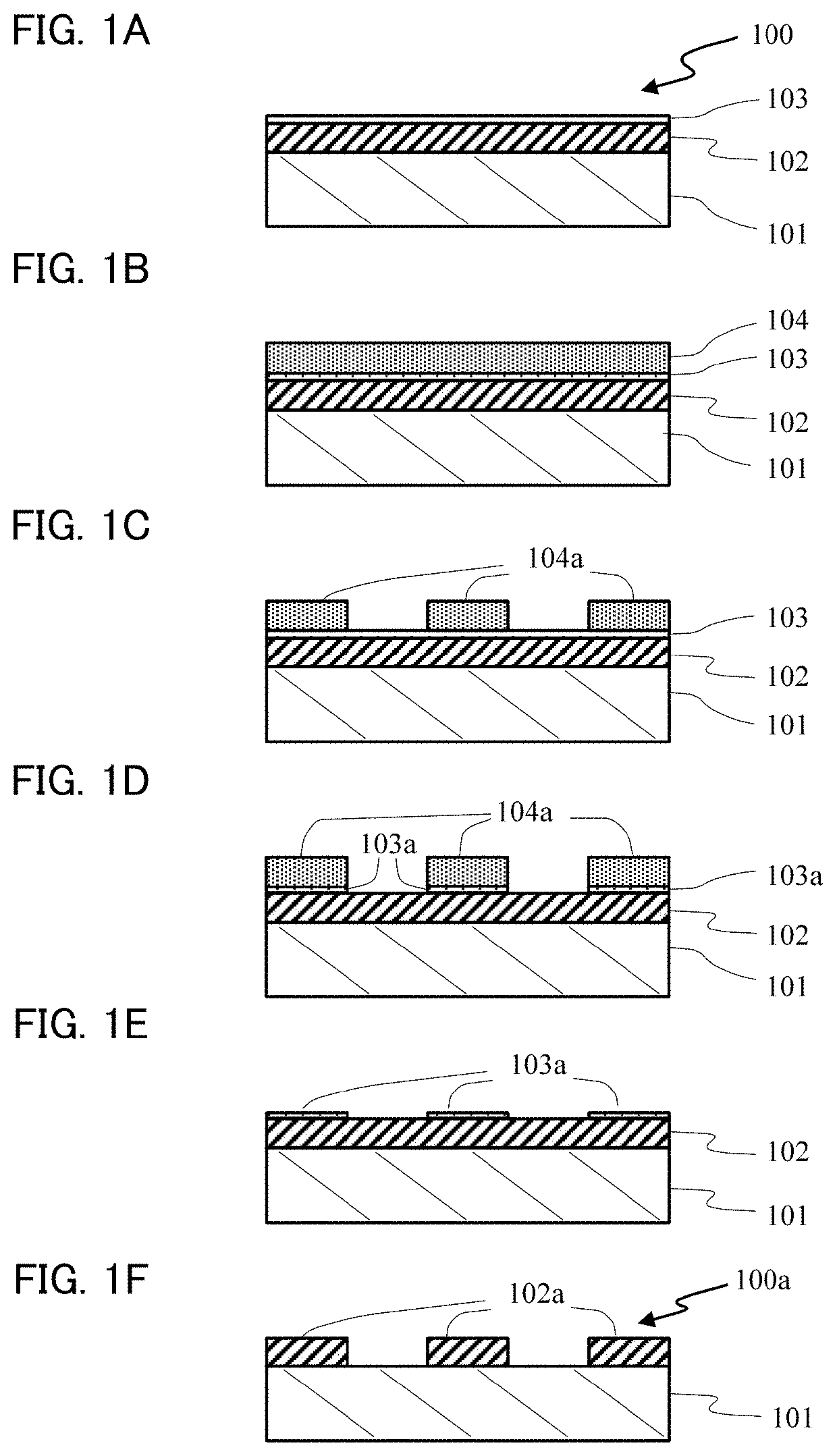
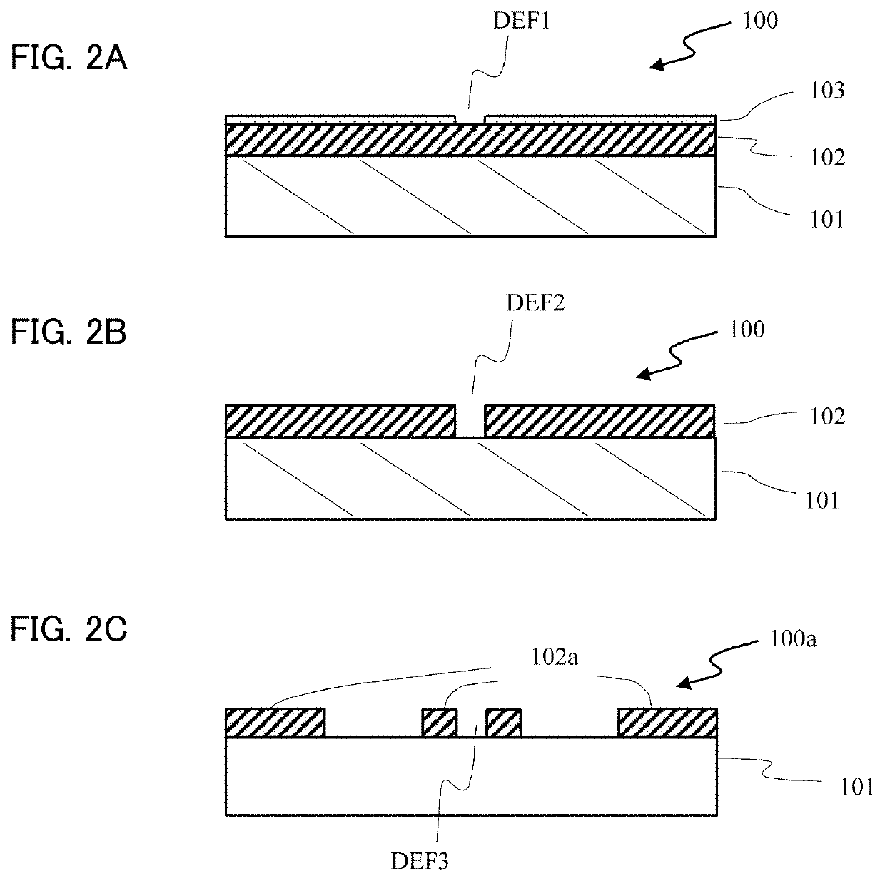
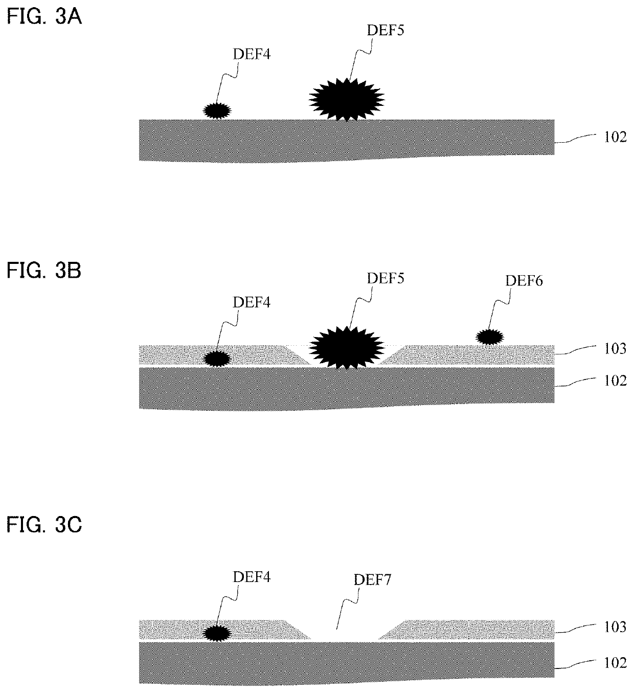
[0093]An undetected defect in an inspection after cleaning was detected and analyzed based on an inspection result before the cleaning after a film is formed in a step of forming SiOx of 10 nm on an outermost surface of a photomask blank. After the film is formed, defects on photomask blanks were inspected using the inspection optical system illustrated in FIG. 4 at a numerical aperture NA of 0.95 and an inspection wavelength of 532 nm before passing through the cleaning step. Positional information on the defect obtained by the inspection was recorded, and the cleaning step was conducted.
[0094]After the photomask blanks were cleaned, defects on the photomask blanks were inspected using an optical inspection apparatus having a numerical aperture NA of 0.85 and an inspection wavelength of 355 nm. Positional information on the defect obtained by the inspection was recorded, and the defect undetected after passing through the cleaning step was extracted by the inspection of a defect be...
PUM
| Property | Measurement | Unit |
|---|---|---|
| thickness | aaaaa | aaaaa |
| thickness | aaaaa | aaaaa |
| wavelength | aaaaa | aaaaa |
Abstract
Description
Claims
Application Information