Magnetoresistive element and magnetic storage device

a magnetic storage device and magnetoresistive element technology, applied in the direction of electrical apparatus, semiconductor devices, galvano-magnetic material selection, etc., can solve the problems of difficult mass production, difficult to put into practical use, and fixed layer is not thermodynamically stable, etc., to achieve excellent tunnel magnetoresistive ratio, and high speed

Pending Publication Date: 2022-10-06
TOHOKU UNIV
View PDF0 Cites 0 Cited by
  • Summary
  • Abstract
  • Description
  • Claims
  • Application Information

AI Technical Summary

Benefits of technology

[0024]Since the magnetic storage device according to the present invention has the magnetoresistive element according to the present invention having an excellent tunnel magnetoresistive ratio, higher speed can be achieved.
[0025]According to the present invention, it is possible to provide a magnetores

Problems solved by technology

The magnetoresistive element described in NPL 5 has an excellent tunnel magnetoresistive ratio, but the Co-film having the bcc structure constituting the free layer and the fixed layer is not a thermodynamically stable structure.
Thus, it is necessary to deposit a Co film of less than 1 nanometer on a Fe thick film as a base, and th

Method used


Image

  • Magnetoresistive element and magnetic storage device
  • Magnetoresistive element and magnetic storage device
  • Magnetoresistive element and magnetic storage device

Examples


example 1

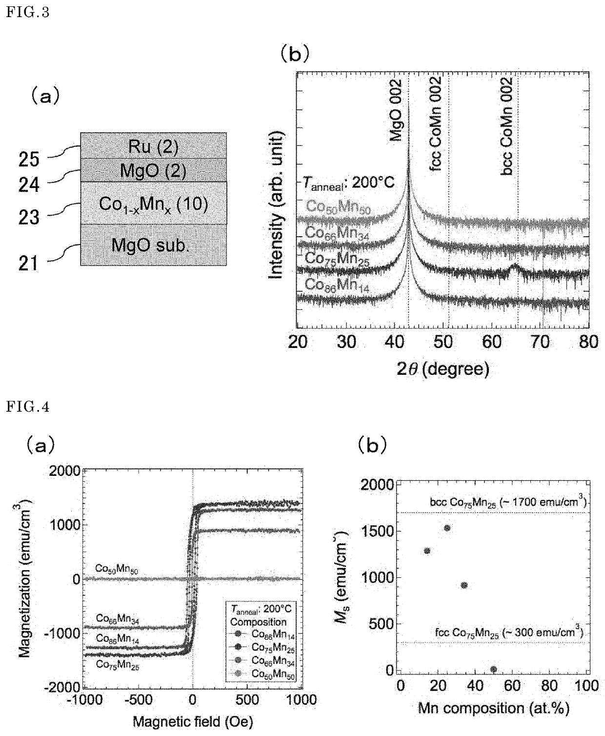
[0048]By sputtering, a magnetic thin film made of an alloy having the bcc structure containing Co as a main component and Co and Mn was manufactured. As illustrated in FIG. 2(a), a Cr layer 22 having a thickness of 40 nm, a CoMn alloy layer 23 made of a Co75Mn25 thin film having a thickness of 10 nm, an MgO layer 24 having a thickness of 2 nm, and an Ru layer 25 having a thickness of 2 nm were sequentially formed on an MgO substrate 21 by sputtering to manufacture a test device. Using the manufactured test device, crystal structure analysis and measurement of magnetization curve (M-H curve) were performed by the X-ray diffraction (XRD) method. The results are illustrated in FIGS. 2(b) and 2(c), respectively.

[0049]As illustrated in FIG. 2(b), in the XRD spectrum, in addition to the peaks corresponding to MgO and Cr, peaks were observed at positions corresponding to CoMn in the bcc structure. In addition, no peak was observed at the position corresponding to the fcc (face-centered cub...

example 2

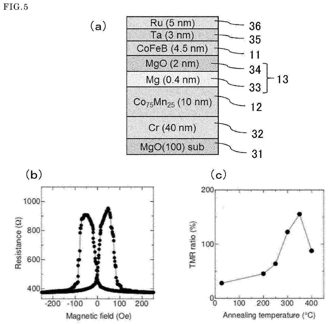
[0055]By sputtering, a magnetoresistive element 10 in which only the free layer is made of a CoMn alloy having the bcc structure was manufactured. As illustrated in FIG. 5(a), a Cr layer (base layer) 32 having a thickness of 40 nm, a second magnetic layer 12 (free layer) made of a Co75Mn25 thin film having a thickness of 10 nm, a non-magnetic layer 13 made of an Mg film 33 having a thickness of 0.4 nm and an MgO film 34 having a thickness of 2 nm, a first magnetic layer 11 (reference layer) made of a CoFeB thin film having a thickness of 4.5 nm, a Ta layer 35 having a thickness of 3 nm, and a Ru layer 36 having a thickness of 5 nm were sequentially formed on an MgO substrate 31 by sputtering, and then subjected to annealing for 1 hour at a predetermined temperature up to 400° C. to manufacture a test device of the magnetic resistance element 10. The annealing temperature of each test device is 25° C. (without annealing), 200° C., 250° C., 300° C., 350° C., and 400° C.

[0056]The tunne...

example 3

[0058]By sputtering, a magnetoresistive element 10 in which both the free layer and the reference layer were made of a CoMn alloy having the bcc structure was manufactured. As illustrated in FIG. 6A, a Cr layer (base layer) 32 having a thickness of 40 nm, a second magnetic layer 12 (free layer) made of a Co75Mn25 thin film having a thickness of 10 nm, a non-magnetic layer 13 made of an MgO film having a thickness of 2.4 nm, a first magnetic layer 11 (reference layer) made of a Co75Mn25 thin film having a thickness of 4 nm, a CoFe layer 37 having a thickness of 1.5 nm, an IrMn layer 38 having a thickness of 10 nm, and a Ru layer 36 having a thickness of 5 nm were sequentially formed on an MgO substrate 31 by sputtering, and then subjected to annealing for 1 hour at a predetermined temperature up to 375° C. to manufacture a test device of the magnetic resistance element 10. The annealing temperature of each test device is 25° C. (without annealing), 250° C., 300° C., 325° C., 350° C.,...


PUM


Abstract

A magnetoresistive element that has a magnetic material made of an alloy having a stable bcc structure containing Co as a main component, has an excellent tunnel magnetoresistive ratio, and can be put into practical use by mass production, and a magnetic storage device using the magnetoresistive element are provided. The magnetoresistive element includes a first magnetic layer whose magnetization direction is substantially fixed, a second magnetic layer whose magnetization direction is changeable, and a non-magnetic layer arranged between the first magnetic layer and the second magnetic layer. The first magnetic layer and/or the second magnetic layer has an alloy having a bcc structure containing Co as a main component and Co and Mn.

Description

FIELD OF THE INVENTION[0001]The present invention relates to magnetoresistive elements and magnetic storage devices.DESCRIPTION OF RELATED ART[0002]In products such as magnetic sensors and non-volatile magnetoresistive memories, magnetoresistive elements that exhibit the so-called tunnel magnetoresistance (TMR) effect are often used. This magnetoresistive element has a three-layer structure in which a magnetic layer (free layer) whose magnetization direction can be changed, a non-magnetic layer (insulating layer), and a magnetic layer (reference layer or fixed layer) whose magnetization direction is substantially fixed are deposited by magnetic tunnel junction, and exhibits a TMR effect in which the electrical resistance changes depending on the magnetization direction of the free layer. The magnitude of this TMR effect is represented by the tunnel magnetoresistive ratio (TMR ratio), which indicates the rate of change of the electrical resistance of the magnetoresistive element.[000...

Claims


Application Information

Patent Timeline
IPC IPC(8): H01L43/10H01L27/22H01L43/02
CPCH01L43/10H01L27/228H01L43/02H01L27/105H10B61/22H10N50/85H10N50/10H10N50/01H10B99/00H10N50/80
Inventor MIZUKAMI, SHIGEMITSUCHIYA, TOMOKIKUNIMATSU, KAZUMAICHINOSE, TOMOHIRO
Owner TOHOKU UNIV
Why Eureka
Try Eureka