

Multispectral semiconductor resonant-cavity detector sensitive in at least two wavelength bands
a multi-spectral semiconductor and resonant cavity technology, applied in the field of multi-spectral semiconductor resonant cavity detector sensitive in at least two wavelength bands, can solve the problems of limited detector efficiency, slow device operation, and large active thickness of devices
- Summary
- Abstract
- Description
- Claims
- Application Information
AI Technical Summary
Problems solved by technology
Method used
Image

Examples
Embodiment Construction
The purpose of this invention is to overcome the above disadvantages.
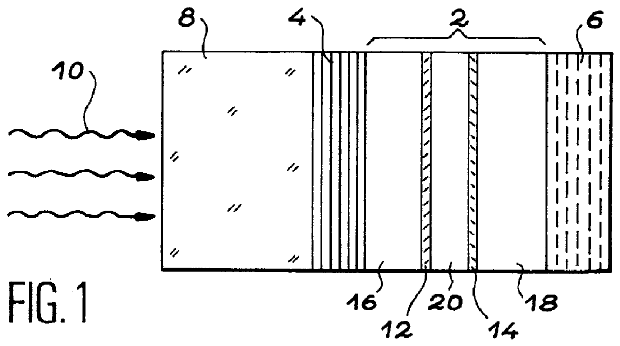
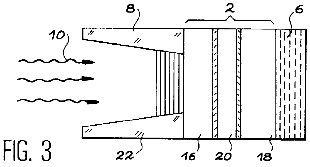
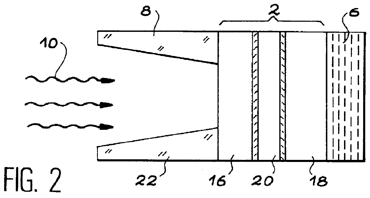
Its purpose is a multispectral detector that comprises at least one resonant cavity in thin layers and in which the colors are electrically separated at each resonant cavity.
Each resonant cavity is designed to resonate at two or more wavelengths.
In each cavity, the fact that stationary waves specific to the different resonant wavelengths are set up, is used to separate these wavelengths.
Consequently, absorbent layers are placed on antinodes specific to these stationary waves.
P-N junctions that contain absorbent layers in their space charge areas, collect the photocurrent generated by the light.
A detector conform with the invention may comprise a set of resonant cavities forming a detection matrix, each resonant cavity corresponding to a pixel.
The precise purpose of this invention is a multispectral detector, characterized in that it comprises at least one resonant cavity designed to resonate at at least two wavelen...
PUM
 Abstract
Description
Claims
Application Information