Off chip driver (OCD) with variable drive capability for noise control

a variable drive and off-chip driver technology, applied in logic circuit coupling/interface arrangement, power consumption reduction, pulse technique, etc., can solve the problems of switching noise, high current change rate (di/dt) in the supply line, and the noise of the power supply line in the integrated circuit (ic) package is well known

Inactive Publication Date: 2000-01-11
IBM CORP
View PDF22 Cites 8 Cited by
  • Summary
  • Abstract
  • Description
  • Claims
  • Application Information

AI Technical Summary

Problems solved by technology

Switching noise on power supply lines in Integrated Circuit (IC) packages is a well known problem.
Typically, switching noise is the result of a high rate of change of current (di / dt) in the supply line.
Consequently, regardless of how small L is made, eventually, as the number of simultaneously switching OCDs increases, switching noise can become unacceptable.
This prior art technique requires very sensitive OCD timing because, the logic signal must begin (e.g., rise) in anticipation of the change in data and last (remain high) until the on device is turned off, without substantially delaying turning on the off device and, thereby, unduly slowing the output transition.
This prior art noise reduction technique also slows forcing tri-state OCDs into their high impedance state.

Method used


Image

  • Off chip driver (OCD) with variable drive capability for noise control
  • Off chip driver (OCD) with variable drive capability for noise control
  • Off chip driver (OCD) with variable drive capability for noise control

Examples


Embodiment Construction

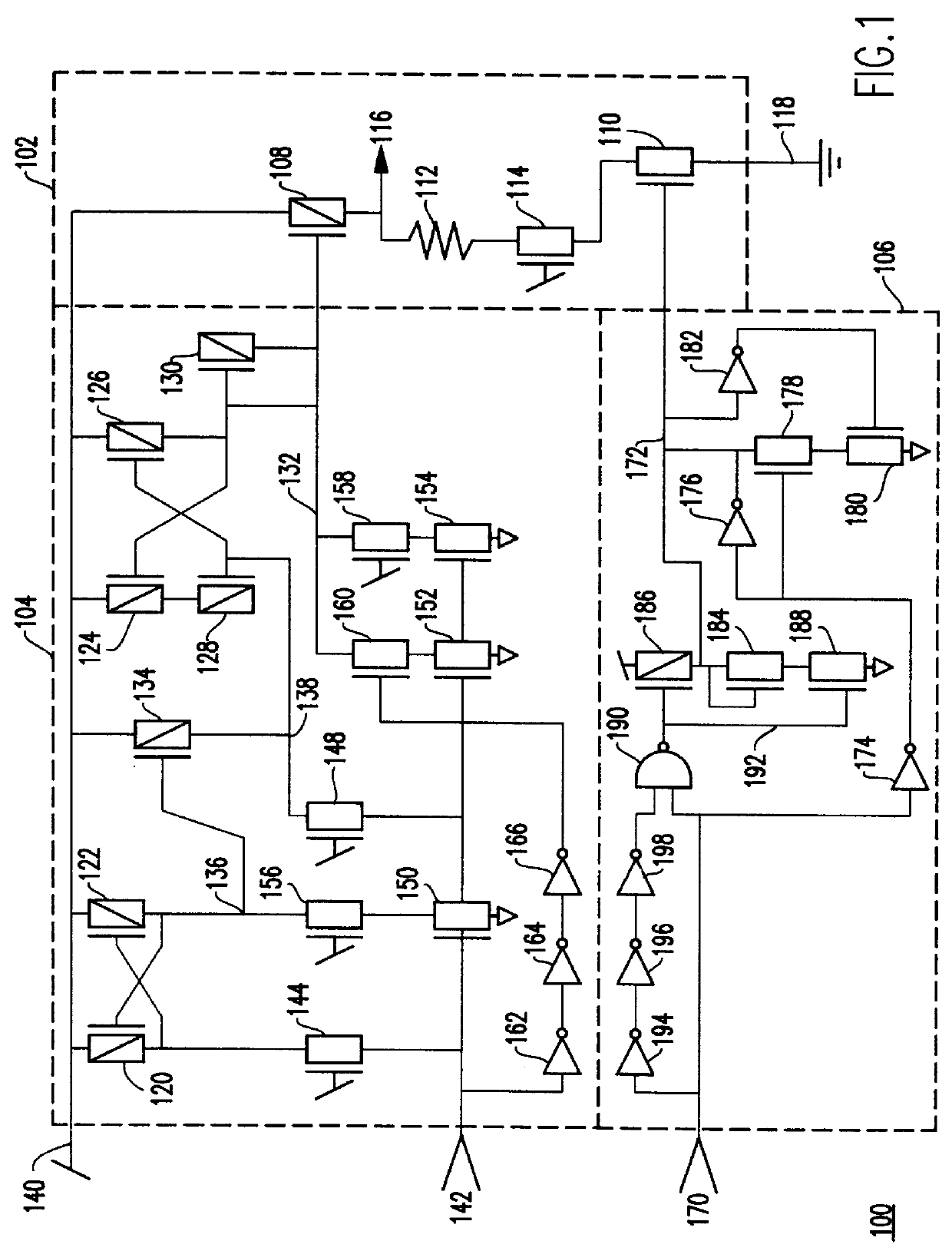
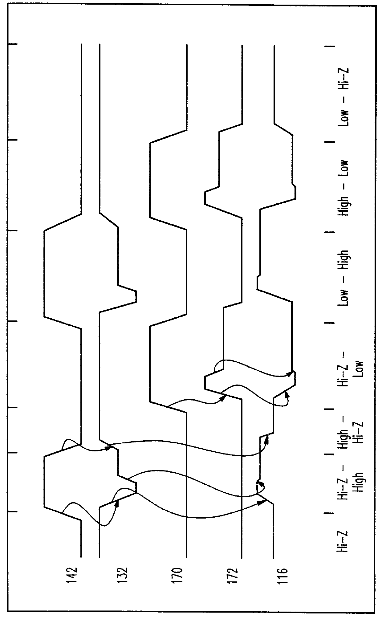
FIG. 1 is a schematic of a first preferred embodiment OCD 100 with self regulating switching current. The OCD includes a Driver 102, an Up-level Pre-drive 104 and a Down-level Pre-drive 106. Driver 102 drive-current mirrors and is controlled by Pre-driver current. The Pre-drive circuits 104, 106 each have an unbalanced input-dependent delay to quickly turn off / on both the on and off driver devices and, after a delay, reduce the drive on the turned on device to a steady state level.

The Driver 102 includes a Pull-up Field Effect Transistor (FET) 108 and a Pull-down FET 110. Preferably, an optional current limiting resistor 112 and punch-through protection FET 114 also are included. Driver FETs 108, 110 and 114 are typically at least 20 times wider than any of the other FETs in the OCD 100 and in some cases several hundred times wider. The current limiting resistor 112 is, preferably, ten ohms (10 .OMEGA.). Preferably, the current limiting resistor is tied between output 116 and the dr...


PUM


Abstract

An Off Chip Driver (OCD) having a high, a low and a high impedance (Hi-Z) state. The OCD includes an up-level pre-drive, a down-level pre-drive and a driver. The driver mirrors current in the up-level pre-drive and down-level pre-drive. Both pre-drive circuits have an unbalanced input-dependant delay to quickly turn off / on the on and off driver devices and, after a delay, reduce the drive on the turned on device to a steady state level. The delay may have a fixed length set by an inverter chain or may be dependent upon output voltage.

Description

1. Field of the InventionThe present invention is related to Integrated Circuits and, more particularly, to integrated circuits with Off Chip Drivers having switching noise compensation.2. Background DescriptionSwitching noise on power supply lines in Integrated Circuit (IC) packages is a well known problem. Typically, switching noise is the result of a high rate of change of current (di / dt) in the supply line. The noise is the voltage that develops across parasitic inductance (L) in the supply line. Thus, switching noise is, simply, L(di / dt).Off Chip Drivers (OCDS) are the primary source of switching noise in state of the art IC packages, especially for complementary insulated gate technology (referred to in the art as CMOS) ICs. Each time an OCD switches its output's state, the supply current to the OCD changes from almost no current to a relatively large current and, then, back to almost no current in a few nanoseconds (ns).This OCD switching current is additive. So, several OCDs...

Claims


Application Information

Patent Timeline
Patent Type & Authority Patents(United States)
IPC IPC(8): H03K19/094H03K19/00
CPCH03K19/0013H03K19/09429
Inventor DOUSE, DAVID E.LEWIS, SCOTT C.MAFFITT, THOMAS M.
Owner IBM CORP
Why Eureka
Try Eureka