Feedback method to repair phase shift masks

a transmission mask and phase shift technology, applied in the field of mask repair, can solve the problems of reducing the minimum pattern resolution substantially, reducing the efficiency of repairing masks, and utilizing time-consuming trial and error methods

Inactive Publication Date: 2000-01-18
GOOGLE LLC
View PDF15 Cites 205 Cited by
  • Summary
  • Abstract
  • Description
  • Claims
  • Application Information

AI Technical Summary

Benefits of technology

to provide a method and system for repairing masks which reduces misalignment, overlap geometry transmission and phase errors in patches added to the mask.

Problems solved by technology

As a consequence, any defects present on the mask may be transferred onto the substrate and result in defects in the final desired structure.
When used on alternate transparent areas of the mask, such phase shifters reduce the minimum pattern resolution substantially, as compared to the photo mask method.
Despite the numerous prior art in this area, known methods of repairing phase shift masks utilize time consuming trial and error methods of adding the materials required to effect the repairs to the mask itself.

Method used


Image

  • Feedback method to repair phase shift masks
  • Feedback method to repair phase shift masks
  • Feedback method to repair phase shift masks

Examples


Embodiment Construction

)

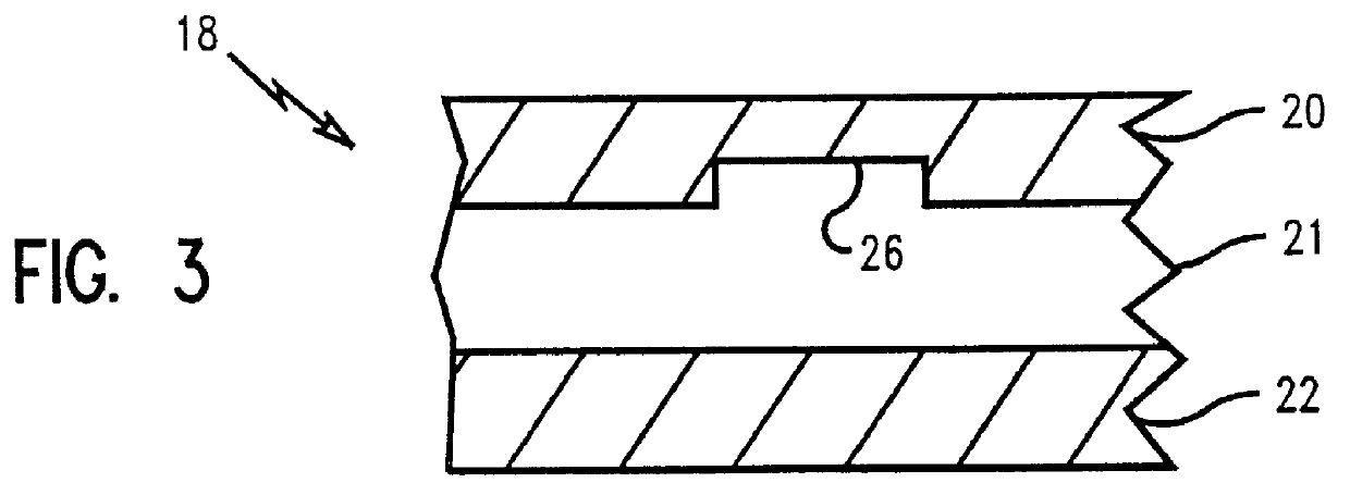
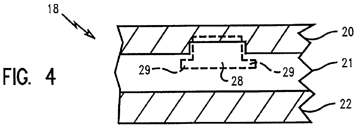
In describing the preferred embodiment of the present invention, reference will be made herein to FIGS. 1-17 of the drawings in which like numerals refer to like features of the invention. Features of the invention are not necessarily shown to scale in the drawings.

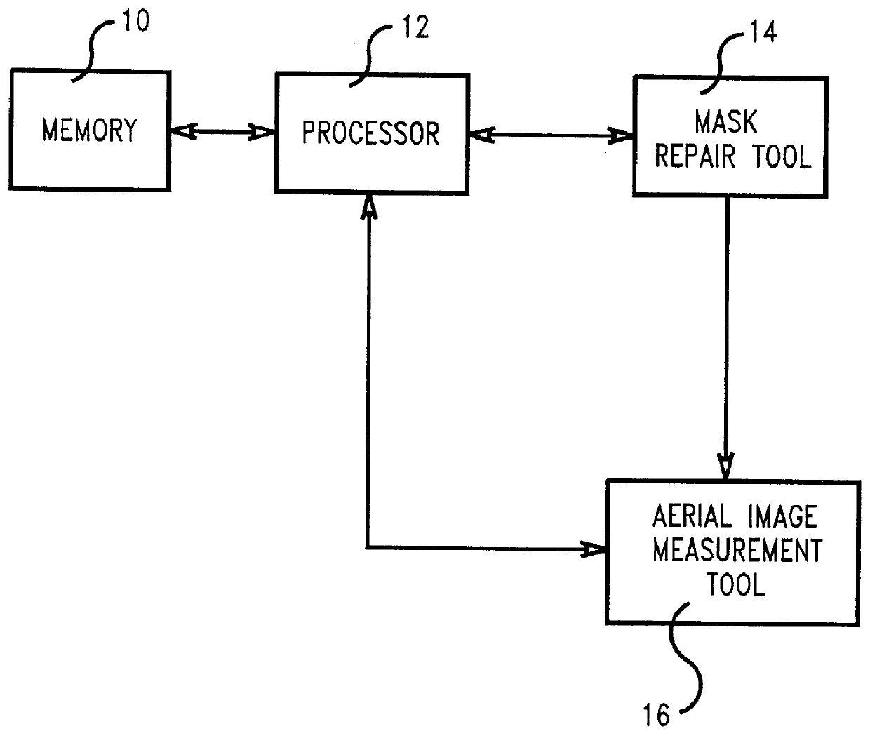
The system utilized in practicing the method of the present invention is depicted in FIG. 1. A mask repair tool is depicted at 14, for example, the repair tool sold by Excel / Quantronix Corp. as DRS model 850. This repair tool preferably comprises ablation and deposition capabilities for chromium and molybdenum silicide. It is also capable of defining various deposition compositions. These deposition compositions will have unique composition and phase characteristics and are repeatable.

Also employed is a device 16 to measure the intensity of the aerial image created by illuminating the mask with the desired light source. A preferred aerial image measurement device is the Microlithography Simulation Microscope 100 AIMS (Ae...


PUM

PropertyMeasurementUnit
thicknessesaaaaaaaaaa
working wavelengthaaaaaaaaaa

Abstract

A method of repairing a semiconductor phase shift mask comprises first providing a semiconductor mask having a defect and then illuminating the mask to create an aerial image of the mask. Subsequently, the aerial image of the mask is analyzed and the defect in the mask is detected from the aerial image. An ideal mask image is defined and compared to the aerial image of the defective mask to determine the repair parameters. Unique parameters for repairing the mask defect are determined by utilizing the aerial image analysis and a look-up table having information on patch properties as a function of material deposition parameters. The mask is then repaired in accordance with the parameters to correct the mask defect. A patch of an attenuated material may be applied to the mask or a predetermined amount of material may be removed from the mask. The aerial image of the repair is analyzed to determine whether the repair sufficiently corrects the defect within predetermined tolerances.

Description

1. Field of the InventionThe present invention relates to a method of repairing a mask for use in lithographic manufacturing of semiconductors and in particular, to a method of repairing phase shift transmission masks.2. Description of Related ArtPhotolithography processes for producing semiconductors and the like utilize masks which are formed by deposition of materials opaque to the light or energy source to be utilized in a desired pattern on a substrate which is generally transparent to such light or energy source (hereinafter referred to generally as light). The mask pattern is transferred via spatially modulated light to create an aerial image which is transferred to a resist film on a substrate. After being exposed to the pattern, the resist film is contacted with a developer and subsequently an etchant to create the desired structure on the substrate.As a consequence, any defects present on the mask may be transferred onto the substrate and result in defects in the final des...

Claims


Application Information

Patent Timeline
Patent Type & Authority Patents(United States)
IPC IPC(8): G03F1/00G03F1/26G03F1/72G03F1/84
CPCG03F1/26G03F1/72G03F1/84
Inventor NEARY, TIMOTHY E.CONRAD, EDWARD W.BULA, OREST
Owner GOOGLE LLC
Why Eureka
Try Eureka