Method for making high-Q inductive elements

a high-q inductive element and inductive element technology, applied in the field of high-q inductive element making, can solve the problems of complex five-level metal silicon technology that is more complicated, and achieve the effects of reducing noise figure, enhancing self-resonant frequency, and reducing nois

Inactive Publication Date: 2000-02-15
MICRON TECH INC
View PDF13 Cites 141 Cited by
  • Summary
  • Abstract
  • Description
  • Claims
  • Application Information

AI Technical Summary

Benefits of technology

enhanced Q factor. It is a further advantage of the present invention that the inductive elements described above have an enhanced self-resonant frequency. It is yet a further benefit of the present invention that the inductive elements described above can be formed in conjunction with standard silicon IC processes.
The inductive elements described above can be incorporated in a receiver and/or a transmitter of a communications systems. As a result, the communications system will exhibit higher selectivity and efficiency, and lower noise figure...

Problems solved by technology

Further, the inductors disclosed in the Burghartz Article require a complex five-level metal sili...

Method used


Image

  • Method for making high-Q inductive elements
  • Method for making high-Q inductive elements
  • Method for making high-Q inductive elements

Examples


Embodiment Construction

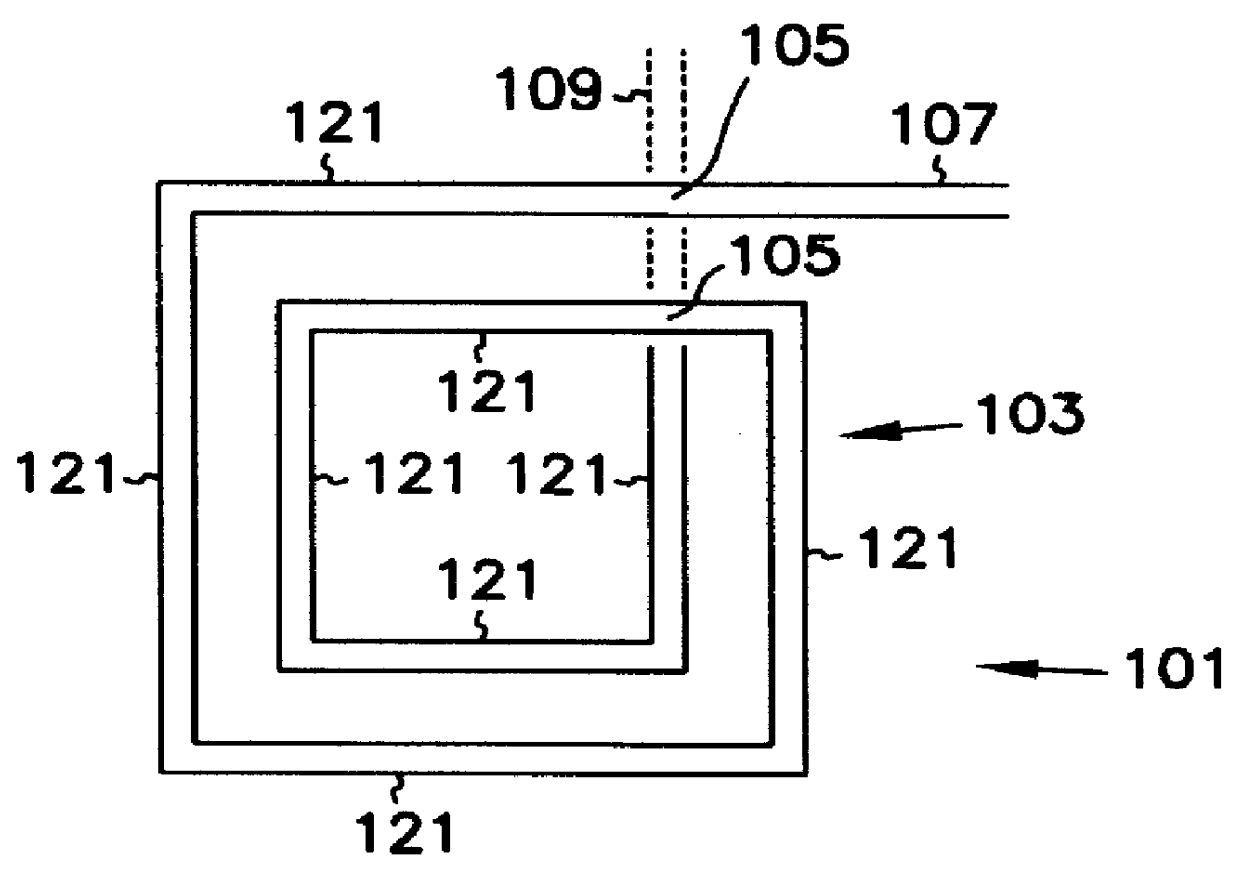
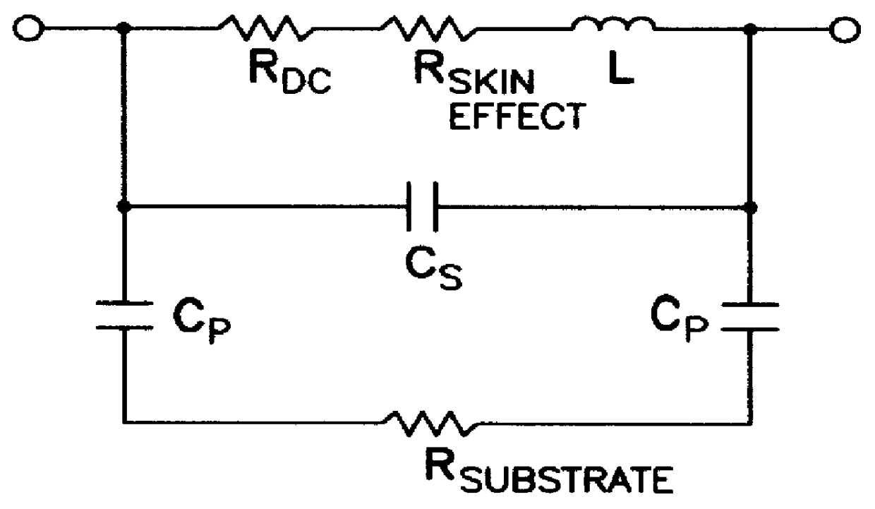
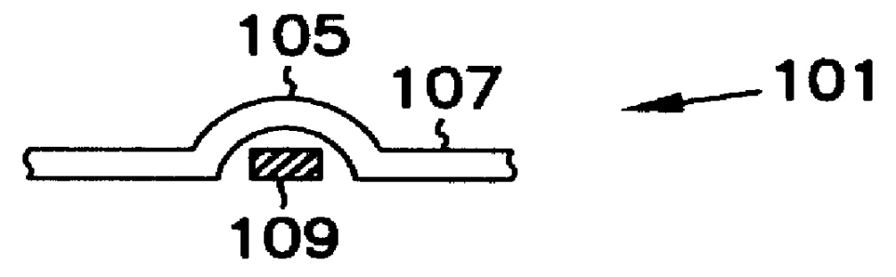
In the following detailed description of the invention, reference is made to the accompanying drawings which form a part hereof, and in which is shown, by way of illustration, specific embodiments in which the invention may be practiced. These embodiments are described in sufficient detail to enable those skilled in the art to practice the invention. Other embodiments may be utilized and structural, logical, and electrical changes may be made without departing from the scope of the present invention. The terms base layer, wafer, and substrate used in the following description include any structure having an exposed surface with which to form the integrated circuit (IC) structure of the invention. The term substrate is understood to include semiconductor wafers. The term substrate is also used to refer to semiconductor structures during processing, and may include other layers that have been fabricated thereupon. Base layer, wafer and substrate include doped and undoped semiconductor...


PUM


Abstract

A first insulator is formed on a base layer. A first conductor is formed on the first insulator. The first conductor is patterned. A second insulator is formed over the first insulator. A via hole is formed in the second insulator and is electrically coupled to the first conductor through the via hole. A second conductor is formed on the second insulator, and is electrically coupled to the first conductor by the via hole. The second conductor is patterned. A cavity is formed under the second conductor, and in the first and second insulators.

Description

The present invention relates generally to integrated circuits, and more specifically to electrical components of integrated circuits.Analog integrated circuits (ICs) are now being extensively used, for example, in wireless radio frequency (RF) applications such as cellular telephones where high frequencies are encountered. Many analog ICs include inductive elements, such as inductors, formed by a conductor. Inductive elements with a relatively high quality (Q) factor, or low loss, are preferably used in analog ICs. As a result, the analog integrated circuits have superior performance, including selectivity, noise figure, and efficiency. Relatively high Q inductors have been formed on insulating bulk semiconductors, such as gallium arsenide.Most integrated circuits, however, are formed on silicon. In comparison to gallium arsenide ICs, silicon ICs can be fabricated relatively inexpensively. Also, analog and digital circuits may be readily combined on silicon ICs. However, unlike gal...

Claims


Application Information

Patent Timeline
IPC IPC(8): H01F41/04H01L21/02H01L27/08
CPCH01F41/041H01L27/08H01L28/10
Inventor FARRAR, PAUL A.FORBES, LEONARD
Owner MICRON TECH INC
Why Eureka
Try Eureka