Array substrate for display device and manufacturing method thereof

a technology of array substrate and display device, which is applied in the direction of picture reproducers, picture reproducers using projection devices, instruments, etc., can solve the problems of reducing manufacturing yield and adversely reducing aperture ratio, and achieves suppressing or eliminating a significant increase in storage capacitor, high aperture ratio, and reduced manufacturing yield

Inactive Publication Date: 2000-02-22
JAPAN DISPLAY CENT INC
View PDF17 Cites 41 Cited by
  • Summary
  • Abstract
  • Description
  • Claims
  • Application Information

AI Technical Summary

Benefits of technology

In accordance with the array substrate and the manufacturing method thereof, since at least the pixel electrode is disposed through the dielectric film(s) with respect to the scanning line and signal line, it becomes possible to locate the pixel electrode sufficiently close to such scanning and signal lines thereby enabling accomplishment of high aperture ratio. Further, the pixel electrode for example is specifically disposed so as to overlap an elongate region as extended from one neighboring scanning line with at least two, first and second dielectric films being laid therebetween; accordingly, even when the overlap region with the pixel electrode increases in area, it will no longer happen that the manufacturing yield is decreased due to occurrence of electrical insulation defects.
Furthermore, with the foregoing arrangement, even on occasions where the overlap region between the pixel electrode and its associative scanning line increases in area, it is possible to suppress or eliminate a significant increase in storage capacitor. More specifically, where the storage capacitor is formed by causing the scanning line and pixel electrode to overlap each other, it will possibly happen that if the storage capacitor is sufficiently great in value, resultant capacitance addition relating to the scanning line increases which in turn leads to an increase in power consumption or to degradation in display performance such as insufficient writing or a decrease in contrast ratio due to a delay in scanning pulse signals. Fortunately, with this invention, even when the periphery of pixel electrode and the elongate region of scanning line are designed to overlap each other in order to define a boundary of pixel electrode for example, the storage capacitor will no longer increase significantly because of the fact that the pixel electrode overlaps the elongate region extended from scanning line with at least two, first and second dielectric films being sandwiched therebetween.

Problems solved by technology

Unfortunately, such storage capacitor line is typically made of optical nontransmissive or opaque materials exhibiting impermeability against light rays, which are generally employed for scanning lines also, in order to eliminate an increase in number of manufacturing process steps required.
The use of such materials may adversely serve to reduce the aperture ratio.
However, such structure does not come without accompanying a problem: electrical interlayer short-circuiting can arise at any overlap sections between scanning lines and pixel electrodes, which in turn leads to a reduction in manufacturing yield.

Method used


Image

  • Array substrate for display device and manufacturing method thereof
  • Array substrate for display device and manufacturing method thereof
  • Array substrate for display device and manufacturing method thereof

Examples


first embodiment

A description will now be given of a liquid crystal display (LCD) device (1) in accordance with a first embodiment of the present invention with reference to FIGS. 1 through 13.

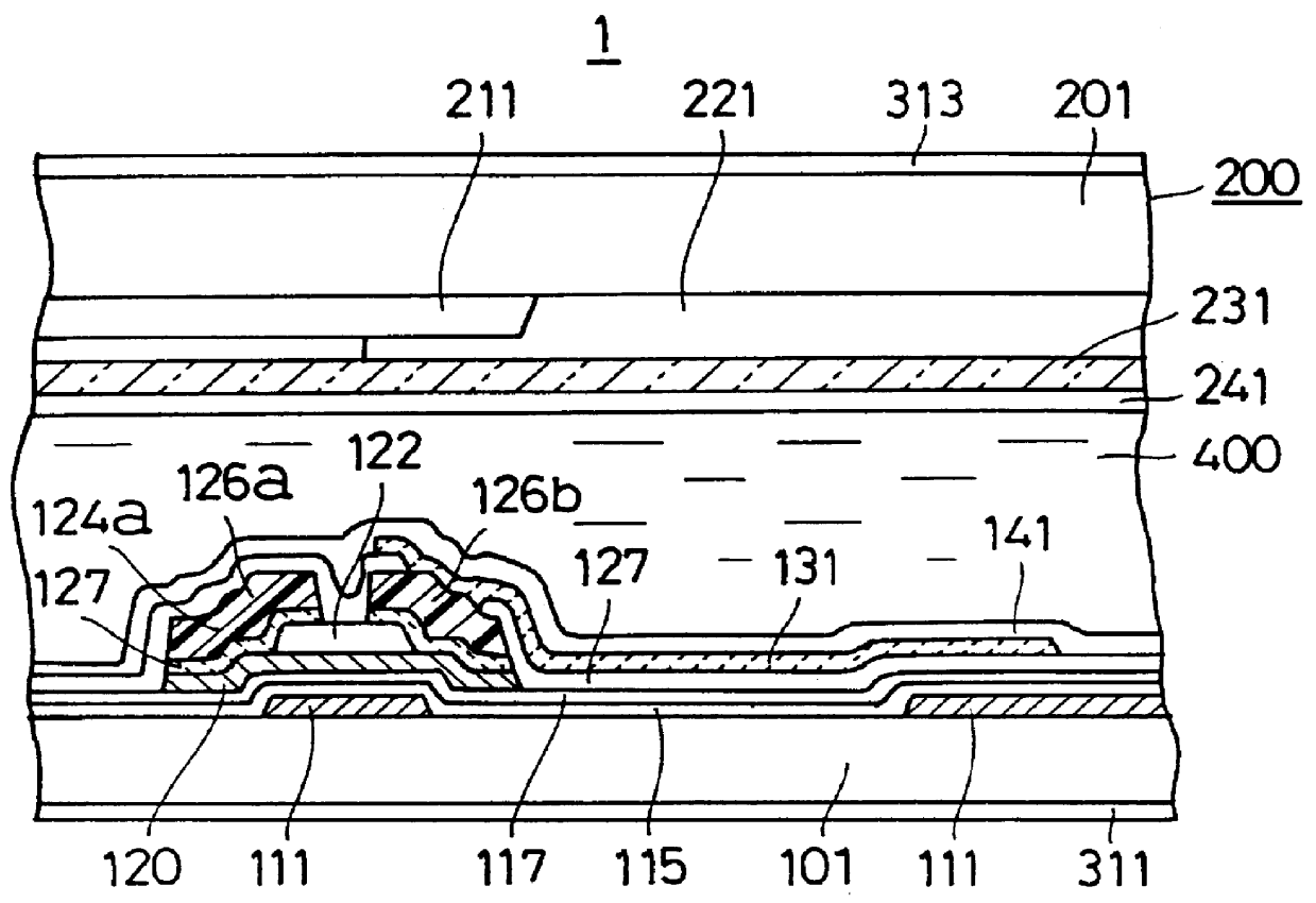
This LCD device (1) is of the light transmissive type capable of displaying color images. As shown in FIG. 2, LCD device (1) has an array substrate (100), an opposed substrate (200), and a twisted nematic (TN) liquid crystal held therebetween through orientation films (141) being laid between it and substrates (100), (200). These orientation films (141), (241) are made of polyimide resin. Also, polarization plates (311), (313) are adhered to the outer surfaces of array substrate (100) and opposed substrate (200), respectively.

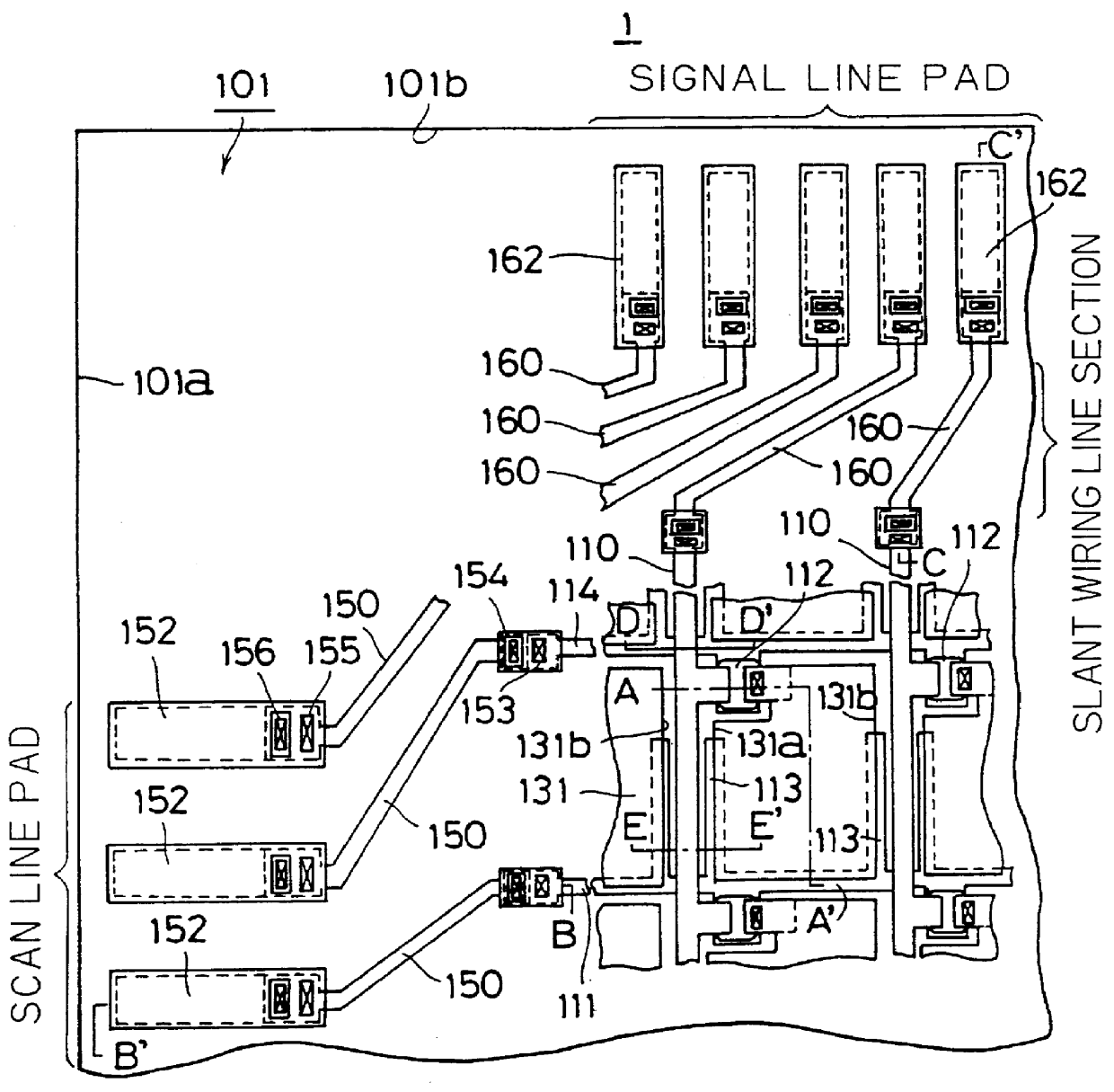
FIG. 1 shows a schematical plan view of the array substrate (100), wherein the lower side of this drawing is to be located at the upper side of the display screen of LCD device (1) while allowing scanning lines to be successively selected in the sequence from the lower to the upper side ...

second embodiment

An optical transmissive LCD device (1) in accordance with a second embodiment of the present invention will be described with reference to FIGS. 15 through 26.

As shown in FIG. 16, LCD device (1) has an array substrate (100), an opposed substrate (200), and a TN liquid crystal held therebetween with an orientation film (141) being laid between it and array substrate (100) and with another orientation film (241) between liquid crystal and opposed substrate (200). These orientation films (141), (241) are made of polyimide resin. Also, polarization plates (311), (313) are adhered to the outer surfaces of array substrate (100) and opposed substrate (200), respectively.

FIG. 15 depicts a schematical plan view of the array substrate (100), wherein the lower side of this drawing is to be located at the upper side of the display screen of LCD device (1) while allowing scanning lines to be successively selected in the sequence from the lower to the upper side of the illustration.

The array subs...

third embodiment

(Advantage of Third Embodiment)

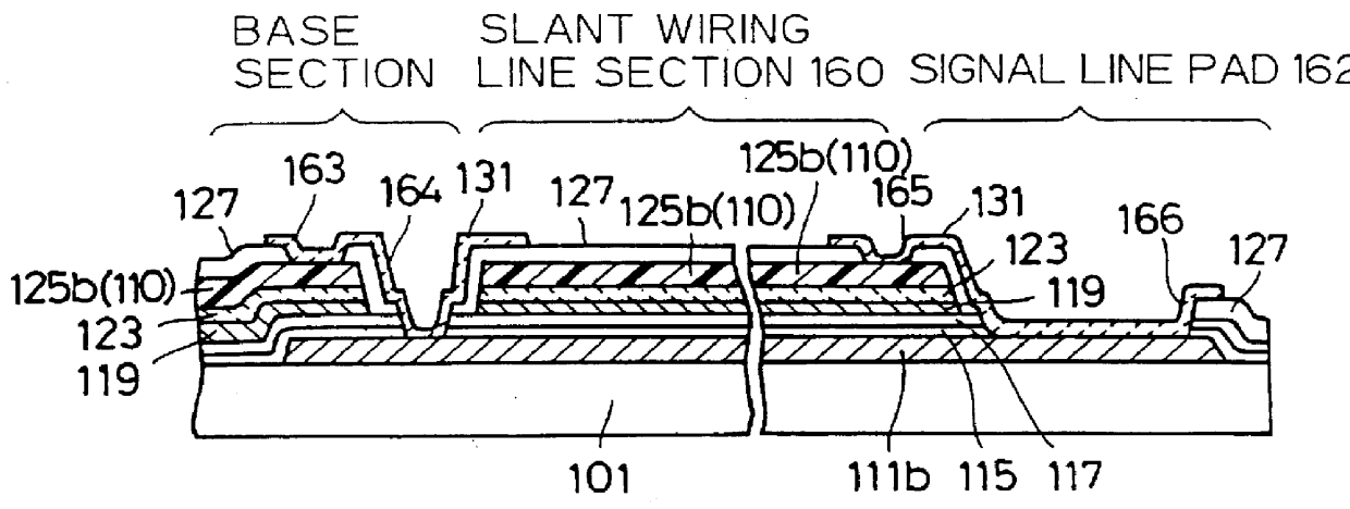
With the array substrate in accordance with the foregoing illustrative embodiment, the array substrate can be formed or manufactured by use of basically five masks. More specifically, an optimized process can be provided for achievement of the conflicting requirements--namely, preventing a reduction in manufacturing yield by miniaturizing any possible step-like differences as caused in wiring lines, and improving the productivity with a decreased number of masks employed therein--as a result of locating the pixel electrodes at the uppermost position, and of employing a specific manufacturing method allowing several process steps to be done simultaneously which steps include: patterning the semiconductor coated films as well as the signal lines, source and drain electrodes at a time using the same mask pattern used therefor; forming the contact holes for interconnection of each source electrode with its associated pixel electrode and the contact holes f...


PUM

PropertyMeasurementUnit
thicknessaaaaaaaaaa
thicknessaaaaaaaaaa
thickaaaaaaaaaa

Abstract

An array substrate includes plural scanning lines (111); a thin film transistor (112) having a first dielectric film (115), (117), a semiconductor film (120) thereon, and a source electrode (126b) electrically coupled to the semiconductor film (120) and a drain electrode (126a); a signal line (110) as taken out of the drain electrode (126a) to extend at substantially right angles to the scanning lines (111); and a pixel electrode (131) electrically connected to the source electrode (126b), wherein the pixel electrode (131) is electrically connected to the source electrode (126b) through a second dielectric film (127) as disposed on at least the signal line (110) while the pixel electrode (131) overlaps an elongate region (113) from its neighboring scanning line (111) through the first and second dielectric films (115), (117), (127). With such an arrangement, an appropriate storage capacitor can be formed by causing the scanning lines and pixel electrode to overlap each other without having to decrease the manufacturing yield while enabling achievement of high aperture ratio.

Description

The present invention relates to array substrates for use in flat panel display devices including liquid crystal display (LCD) devices and the manufacturing method thereof.In the recent years flat panel display devices are more frequently developed to replace conventional cathode-ray tube (CRT) units; in particular, LCD devices are becoming commercially attractive more and more due to their advantage such as light weight, thinness, low power consumption and the like.As one typical prior known LCD devices, an light transmissive active-matrix LCD device will now be described herein which comes with a plurality of switch elements each of which is at a respective one of picture elements. The active-matrix LCD device includes a liquid crystal layer as held between an array substrate and a opposed substrate with orientation films being provided between the liquid crystal layer and any one of such substrates. The array substrate has, on a transparent insulative substrate made of glass, qua...

Claims


Application Information

Patent Timeline
Patent Type & Authority Patents(United States)
IPC IPC(8): G02F1/13G02F1/1362G02F1/1345H01L21/70H01L27/12H01L21/84H01L21/77
CPCG02F1/1345G02F1/13452G02F1/13458G02F1/136213G02F1/136227H01L27/1214G02F2001/13629G02F1/13629H01L27/124H04N9/31
Inventor DOHJO, MASAYUKIKAWANO, HIDEOKUBO, AKIRASHIBUSAWA, MAKOTOIIZUKA, TETSUYANAKAI, TAMIOMORI, KAZUSHIGE
Owner JAPAN DISPLAY CENT INC
Why Eureka
Try Eureka