
Postcharged interconnection speed-up circuit

a technology of post-charge interconnection and speed-up circuit, which is applied in the direction of logic circuit coupling/interface arrangement, logic circuit, pulse technique, etc., can solve the problems of large circuit and additional area overhead, address the use of delay circuit, repeater propagation delay inherent, etc., to achieve small layout area, small propagation delay, and small layout area

Inactive Publication Date: 2000-02-29
THE BOARD OF TRUSTEES OF THE LELAND STANFORD JUNIOR UNIV
View PDF7 Cites 14 Cited by
  • Summary
  • Abstract
  • Description
  • Claims
  • Application Information

AI Technical Summary

Benefits of technology

Accordingly, it is a principal object of the invention to provide a bi-directional repeater circuit with a smaller layout area and a smaller propagation delay than existing circuits, enabling the design of programmable interconnect architectures with smaller layout area, and with smaller propagation delays, than existing ones.
In accordance with the present invention, a speed-up circuit for use in electrically programmable interconnect architectures is disclosed. In a programmable interconnect architecture consisting of a plurality of conductive nodes interconnected by programmable passive switches, this circuit acts as a bi-directional repeater with negligible added propagation delay, and with a minimum redundancy in the number driver transistors, resulting in faster and more area efficient circuits.

Problems solved by technology

However, repeaters have an inherent propagation delay.
The fact that three-state buffers are employed implies large circuits and additional area overhead due to memory cells in the repeaters.
However, that circuit is directed to providing a short propagation delay in a dynamic logic uni-directional carry chain and it does not address the use of a delay circuits for evaluation and for postcharging in order to obtain a circuit that works independent of a clock.
Finally, it does not address the use of such a circuit in a programmable interconnect architecture, and it does not address the use of such a precharge and evaluation circuit for bi-directional signal propagation.
However, that circuit has four network nodes, is not directed to use as a single-terminal circuit for addition to intermediate nodes of an RC tree, and is not directed to use in bi-directional interconnections.
However, that circuit is directed towards reducing the capacitive loading in a uni-directional circuit by using a negative feedback path for postcharging a dynamic logic node, and does not address the use of a positive feedback path to enhance a transition.

Method used


Image

  • Postcharged interconnection speed-up circuit
  • Postcharged interconnection speed-up circuit
  • Postcharged interconnection speed-up circuit

Examples


embodiment 26

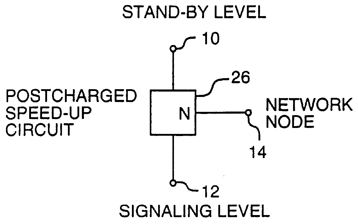
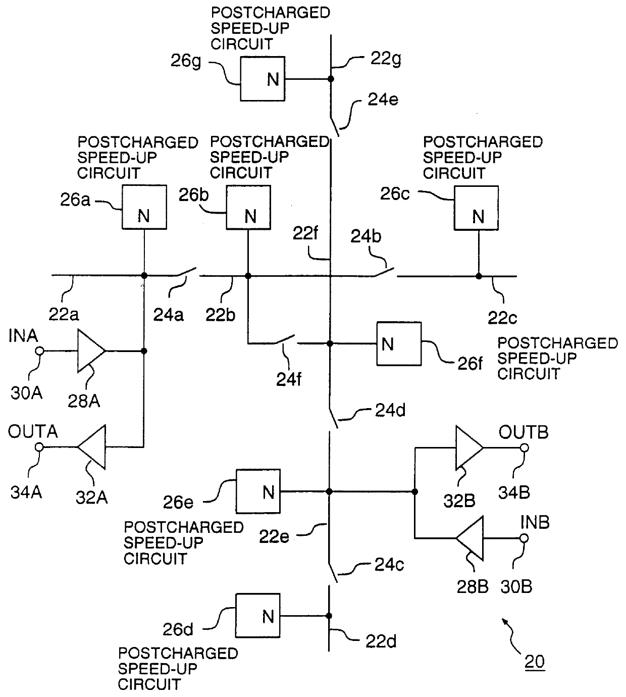
After said first predetermined period of time, each of speed-up circuits 26a, 26b, 26f and 26e in turn goes to the postcharge state, each connecting their network nodes N to the stand-by supply node for said second predetermined period of time, as described for the operation of embodiment 26 of FIG. 1.

Now referring to FIG. 2 again, after said second predetermined period of time, each of speed-up circuits 26a, 26b, 26f and 26e turns to the stand-by state, providing a high impedance at their network nodes N. In this state, conductive leads 22a, 22b, 22f and 22e stay at the stand-by level, due to capacitive charge storage and due to the stand-by level output of buffer 28A.

Hence, pulses at input node 30A are quickly propagated through programmable interconnect architecture 20 and appear on output node 34A. Conversely, pulses at input node 30B are quickly propagated through programmable interconnect architecture 20 and appear on output node 34B. Hence, a circuit style for providing fast,...

embodiment 40

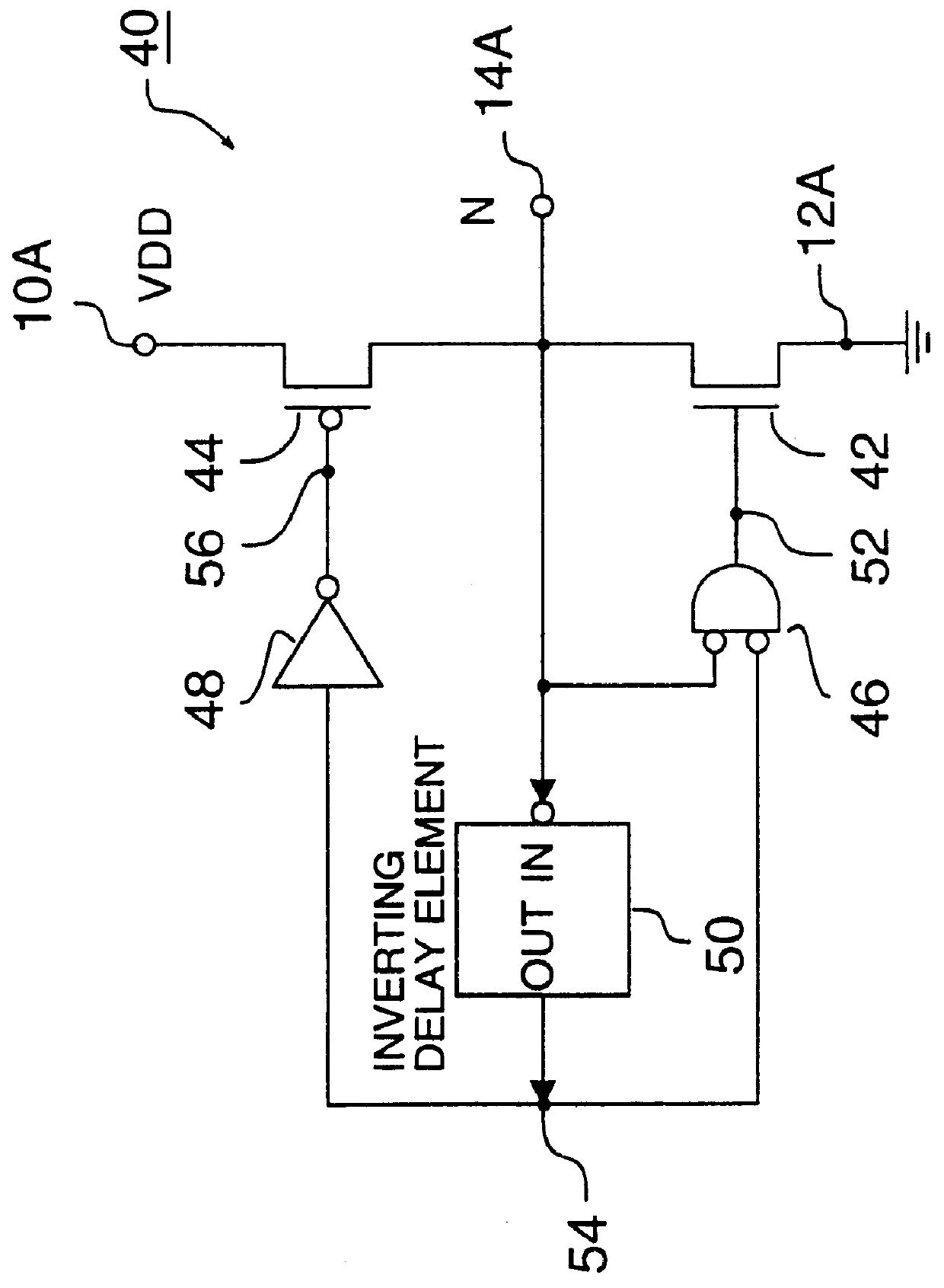
In embodiment 40 of FIG. 3A, weak feedback circuitry to prevent network node 14A from floating while embodiment 40 is in the stand-by mode can consist of a simple inverter with its input connected to network node 14A, and its output connected to the gate of a weak PMOS pull-up transistor, that has its first current terminal connected to stand-by supply node 10A, and its second current terminal connected to network node 14A, as known in the art. It is clear that said simple inverter can be a part of inverting delay element 50.

It is clear that inverting delay element 50 can use known techniques such as the use of an on-chip bias voltage for obtaining a desired delay as a function of environmental and technology parameters.

FIG. 3B shows the schematic of an embodiment 60 of a speed-up circuit according to the present invention. Embodiment 60 comprises a stand-by supply node 10B, a signaling supply node 12B, and a network node 14B. Embodiment 60 further comprises three intermediate nodes...

embodiment 60

In embodiment 60 of a postcharged speed-up circuit according to the present invention, shown in FIG. 3B, the stand-by supply level on stand-by supply node 10A is the negative supply for the circuitry and equals a logic low level, and the signaling supply level on signaling supply node 12A is the positive supply for the circuitry and equals a logic high level. The operation of embodiment 60 is complementary to the operation of embodiment 40, and is as follows. When a low level or stand-by level is present on network node 14B for a sufficiently long period of time, a high level is present at the output of inverting delay element 70, on intermediate node 74. Hence, logic NAND gate 66 has one input at a low level, on network node 14B, and one input at a high level, on intermediate node 74, and hence its output, on intermediate node 72, is high. Therefore, PMOS transistor 62 is off and provides a high impedance equivalent to an open circuit between network node 14B and signaling supply n...


PUM


Abstract

A circuit style, which may be employed in fast, area-efficient, flexible programmable interconnect architectures, or in logic circuits, is disclosed. In one embodiment, a plurality of postcharged speed-up circuits, each having a single network node, is connected to the intermediate nodes of a programmable interconnect architecture. Each speed-up circuit monitors the logic level on the network node. When a circuit detects a substantial change in logic level, away from the stand-by level, it temporarily enforces that change by connecting its network node to the signaling logic level. Thus, on each node, a low-impedance enhancement of the signal driving the node temporarily appears. This causes the potential on neighboring nodes, connected through conducting programmable switches, to change towards the signaling level, and their speed-up circuits in turn temporarily enforce the new level. After the temporary enforcement of the signaling level, each speed-up circuit forces its network node back to the stand-by level, for a predetermined period of time. Thus, a forced pulse away from the stand-by logic level towards the signaling level on a node quickly propagates to its connected nodes.

Description

1. Field of the InventionThe present invention relates to integrated circuit (IC) technology. More specifically, the present invention pertains to fast circuits for realizing programmable interconnect architectures among circuitry on one integrated circuit, and among circuitry on different integrated circuits.2. Prior ArtProgrammable interconnect architectures are used in user-programmable arrays of logic cells, also referred to as "Field Programmable Gate Arrays (FPGAs)", as well as in dedicated programmable interconnect chips, microprocessors, digital signal processor cores, etc.Such programmable interconnect architectures typically consist of a network of conductive nodes, programmable passive switches, and programmable or non-programmable repeater circuits. An interconnection from one conductive node to another is obtained by programming the intermediate passive switches to be conducting, and by programming each repeater circuit to be propagating and enhancing the signal from on...

Claims


Application Information

Patent Timeline
Patent Type & Authority Patents(United States)
IPC IPC(8): H03K19/017H03K19/01
CPCH03K19/01721
Inventor DOBBELAERE, IVO
Owner THE BOARD OF TRUSTEES OF THE LELAND STANFORD JUNIOR UNIV
Learn More