

Semiconductor device manufacturing machine and method for manufacturing a semiconductor device by using the same manufacturing machine
a manufacturing machine and semiconductor technology, applied in the field of semiconductor device manufacturing machines and a manufacturing method by using the same manufacturing machine, can solve the problems of reducing the production yield affecting the production efficiency of the manufacturing machine, and unable to properly compensate the plasma distribution
- Summary
- Abstract
- Description
- Claims
- Application Information
AI Technical Summary
Problems solved by technology
Method used
Image

Examples
first embodiment
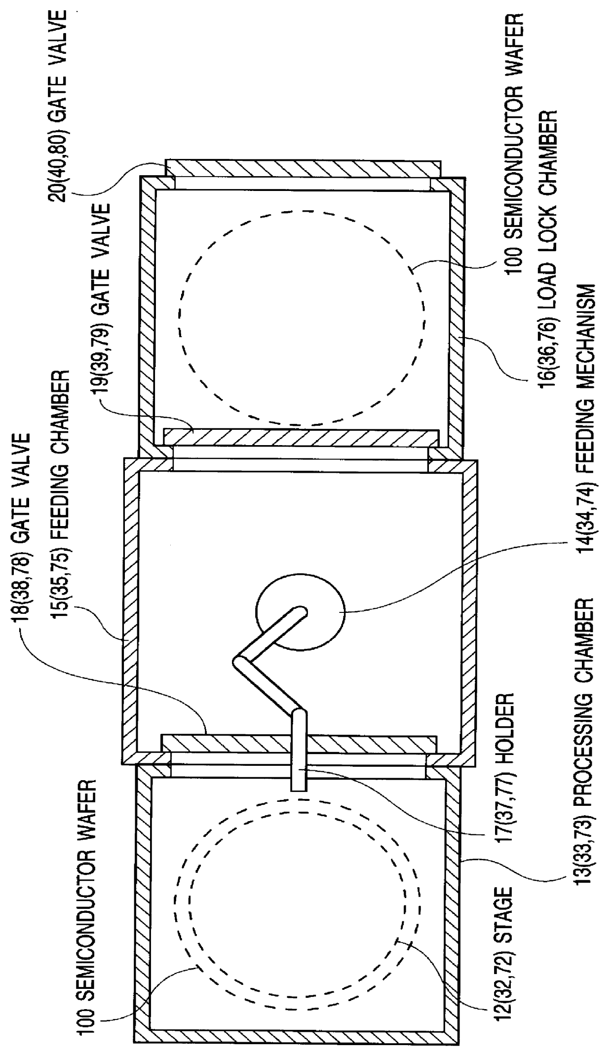
the semiconductor device manufacturing machine in accordance with the present invention is that the present invention is applied to a parallel plate type, single-wafer-processing type, dry etching machine. Therefore, an overall construction of this embodiment is similar to that of the example shown in FIG. 1, and therefore, in place of a drawing showing the overall construction of this embodiment, new Reference Numerals for showing the overall construction of this embodiment are added to FIG. 1.
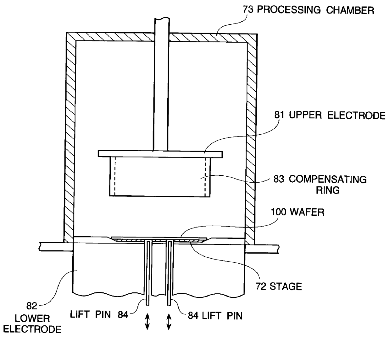
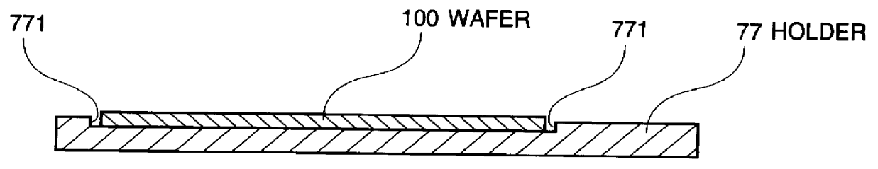
Namely, the first embodiment includes a stage 12, a processing chamber 13, a feeding mechanism 14, a feeding chamber 15, a load lock chamber 16, a holder 17 and gate valves 18 to 20, which are similar to corresponding ones of the prior art example. However, as shown in FIGS. 4 and 5, the processing chamber 13 and the holder 17 are different in a detailed construction from those of the processing chamber 73 and the holder 77 of the prior art shown in FIGS. 2 and 3.
The processing chamber 13 as ...
embodiment 2
Now, a second embodiment of the semiconductor device manufacturing machine in accordance with the present invention and a second embodiment of the semiconductor device manufacturing method in accordance with the present invention using the second embodiment of the semiconductor device manufacturing machine will be described.
second embodiment
the semiconductor device manufacturing machine in accordance with the present invention is that the present invention is applied to a sputtering machine. However, an overall construction of this second embodiment is similar to that of the parallel plate type, single-wafer-processing type, dry etching machine shown in FIG. 1, and therefore, in place of a drawing showing the overall construction of this second embodiment, new Reference Numerals for showing the overall construction of this second embodiment are added to FIG. 1.
Namely, the second embodiment includes a stage 32, a processing chamber 33, a feeding mechanism 34, a feeding chamber 35, a load lock chamber 36, a holder 37 and gate valves 38 to 40, which are similar to corresponding ones of the prior art example. However, as shown in FIGS. 10 and 11, the processing chamber 33 and the holder 37 are different in a detailed construction from those of the processing chamber 73 and the holder 77 of the prior art shown in FIGS. 2 an...
PUM
| Property | Measurement | Unit |
|---|---|---|
| pressure | aaaaa | aaaaa |
| atmospheric pressure | aaaaa | aaaaa |
| vacuum level | aaaaa | aaaaa |
Abstract
Description
Claims
Application Information