Method and apparatus of monitoring polishing pad wear during processing

a technology of polishing pad and polishing surface, applied in the field of method and apparatus, can solve the problems of reducing the polishing removal rate, affecting the removal of a quantity of pad material, and reducing the uniformity of polishing removal, so as to reduce the degradation of polishing pad uniformity

Inactive Publication Date: 2000-04-04
IBM CORP
View PDF13 Cites 86 Cited by
  • Summary
  • Abstract
  • Description
  • Claims
  • Application Information

AI Technical Summary

Benefits of technology

It is another object of the present invention to provide a method and apparatus of the type described which utilizes a closed-loop feedback process to control the chemical-mechanical polishing in real time in order to minimize the degradation in polishing pad uniformity.
It is yet another object of the present invention to provide a method and apparatus of the type described which can detect the release of a semiconductor wafer from the chemical-mechanical polishing tool wafer carrier during polishing.

Problems solved by technology

This diminishes the polishing removal rate and degrades the polishing removal uniformity.
While conditioning of the pad surface improves polishing uniformity and rates, it has the detrimental effect of removing a quantity of pad material.
If the abrasion of the pad material is not. uniform across the pad surface that contacts the wafer, the polishing uniformity and the pad's useful lifetime will be adversely affected.
When this occurs, the polishing process subjects the unrestrained wafer to damage.
Presently, the only ways available to measure the pad material removal are destructive to the pad; cutting a piece from the pad and using a micrometer to measure thickness, or contacting the pad using a micrometer and a straightedge across the pad surface.
Thus, pad destruction or pad contamination may result from measurements currently made in the prior art.
However, the non-uniformity of polishing pad material removal is not addressed, as the polishing pad thickness or its relative change is not measured or monitored.
However, this passive acoustical technique deals with a method of polishing and monitoring for end point detection on the semiconductor wafer, not a method for monitoring or measuring a change in the polishing pad thickness.
Nor does this technique employ an active radiation source in its measurement scheme.
Although the general measurement technique utilizes reflected radiation, beam intensity is the sole operational parameter, not an interferometer technique utilizing phase change or time delay.
Also, once again, the polishing pad itself is not monitored or measured in this prior art.

Method used


Image

  • Method and apparatus of monitoring polishing pad wear during processing
  • Method and apparatus of monitoring polishing pad wear during processing

Examples


Embodiment Construction

)

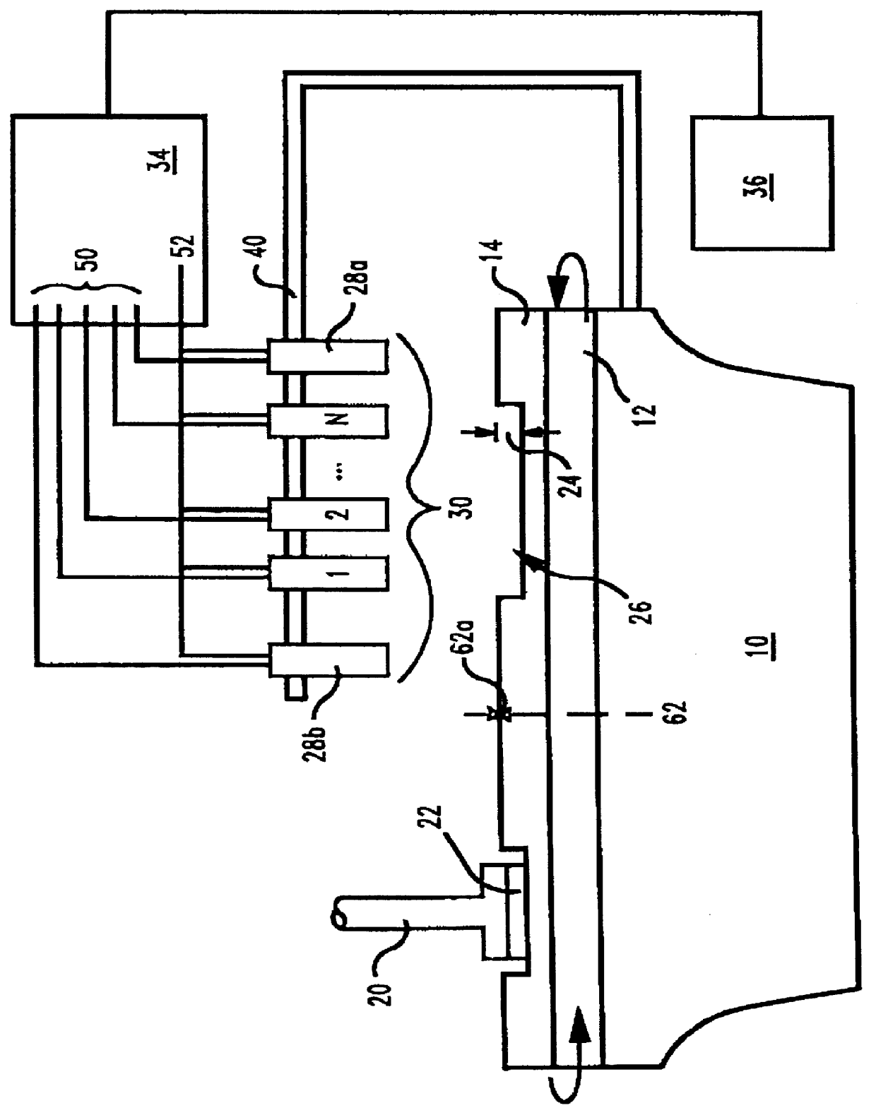
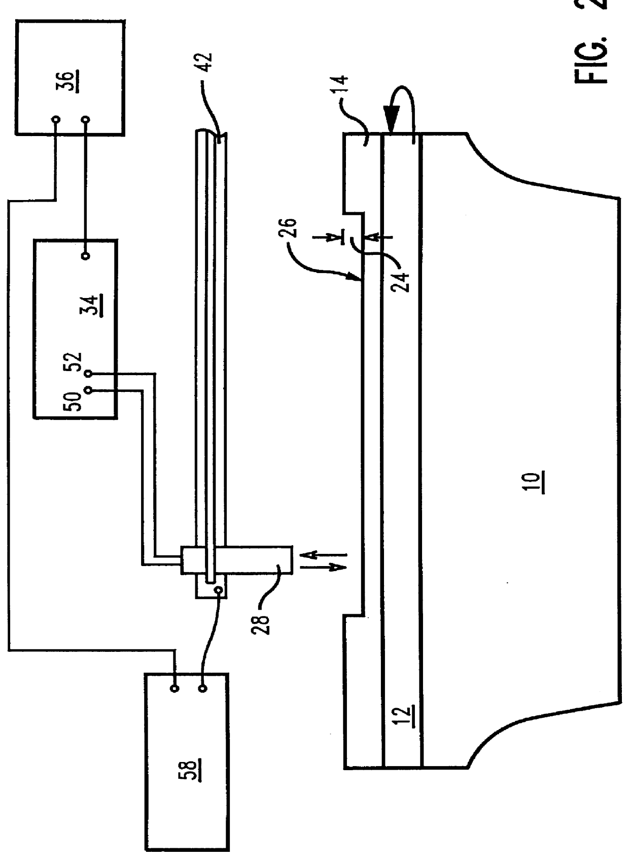
In describing the preferred embodiment of the present invention, reference will be made herein to FIGS. 1 and 2 of the drawings in which like numerals refer to like features of the invention. Features of the invention are not necessarily shown to scale in the drawings.

The present invention addresses the problems associated with the prior art of: a) removing polishing pad material in an unregulated, non-uniform manner; b) extending the polishing pad's useful life; c) maintaining and improving polishing pad uniformity throughout the chemical-mechanical polishing process; d) performing pad monitoring without damaging the pad surface; and, e) sensing when wafers being polished come off the wafer carrier and remain on the polishing table.

This is accomplished in the present invention by measuring and monitoring the diminished pad thickness using a non-intrusive, non-contacting measurement system, and creating a closed-loop system for adjusting the chemical-mechanical polishing tool's pro...


PUM

PropertyMeasurementUnit
thicknessaaaaaaaaaa
softaaaaaaaaaa
flatnessaaaaaaaaaa

Abstract

A method and apparatus for monitoring polishing pad wear during processing is developed to extend the pad's useful life, and maintain pad uniformity. This is accomplished in the present invention by measuring and monitoring the diminished pad thickness using a non-intrusive measurement system, and creating a closed-loop system for adjusting the chemical-mechanical polishing tool process parameters. The non-intrusive measurement system consists of an interferometer measurement technique utilizing ultrasound or electromagnetic radiation transmitters and receivers aligned to cover any portion of the radial length of a polishing pad surface. The measurement system is sensitive to relative changes in pad thickness for uniformity, and to abrupt changes such as detecting wafer detachment from the CMP wafer carrier.

Description

1. Field of the InventionThe present invention relates generally to semiconductor wafer processing techniques using chemical-mechanical polishing, and more particularly to methods and apparatus for measuring the removal of material from a polishing pad.2. Description of Related ArtDuring the manufacture of integrated circuits it is necessary to polish a thin wafer of semiconductor material in order to remove material and dirt from the wafer surface. Typically, a wet chemical abrasive or slurry is applied to a motor driven polishing pad while a semiconductor wafer is pressed against it in a process well known in the prior art as chemical-mechanical polishing (CMP). The polishing platen is usually covered with a soft wetted material such as blown polyurethane. The polishing effects on the wafer result from both the chemical and mechanical action.The polishing pad contacts the wafer surface while both wafer and pad are rotating on different axes. The rotation facilitates the transport ...

Claims


Application Information

Patent Timeline
Patent Type & Authority Patents(United States)
IPC IPC(8): B24B49/00B24B37/005
CPCB24B49/183B24B37/005B24B49/02
Inventor FISHER, JR., THOMAS R.JASO, MARK A.STEVENS, JR., LEONARD C.
Owner IBM CORP
Why Eureka
Try Eureka