Method of producing planar metal-to-metal capacitor for use in integrated circuits

a technology of metal-to-metal capacitors and integrated circuits, which is applied in the direction of capacitors, semiconductor devices, electrical apparatus, etc., can solve the problems of inability to control the residues and surface texture on the top of the lower metal plate, and the current process is not robust and reliabl

Inactive Publication Date: 2000-05-30
GLOBALFOUNDRIES INC
View PDF18 Cites 38 Cited by
  • Summary
  • Abstract
  • Description
  • Claims
  • Application Information

AI Technical Summary

Benefits of technology

According to the invention, a new method of forming metal-to-metal capacitors provides a simpler process which has a better yield and more reliable structure by creating a metal-to-metal capacitor on a planar surface, not in deep trenches. In addition to the process simplicity, the new method also allows the use of any dielectric materials which are needed by the product designer; e.g., higher or lower dielectric constant and also not limited by high etch rate difference. Because the inventive process is a planar process, there are no corners in the bottom of deep trenches to cause yield and reliability problems. The capacitor area can be adjusted to any shape because there are no edge effects.

Problems solved by technology

The primary drawback of such a capacitor structure is the trade off in thickness of the TD layer 16.
The current process is not a robust reliable process because (a) it requires conformal deposition of a thin dielectric film into narrow gaps at high aspect ratios, (b) it is difficult to control residues and surface texture on top of the lower metal plate and on the sidewalls of the trough, and (c) the process must be integrated with the stud deposition process and its associated cleans.
Because the inventive process is a planar process, there are no corners in the bottom of deep trenches to cause yield and reliability problems.

Method used


Image

  • Method of producing planar metal-to-metal capacitor for use in integrated circuits
  • Method of producing planar metal-to-metal capacitor for use in integrated circuits
  • Method of producing planar metal-to-metal capacitor for use in integrated circuits

Examples


Embodiment Construction

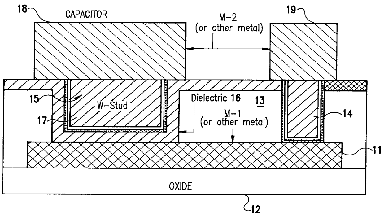
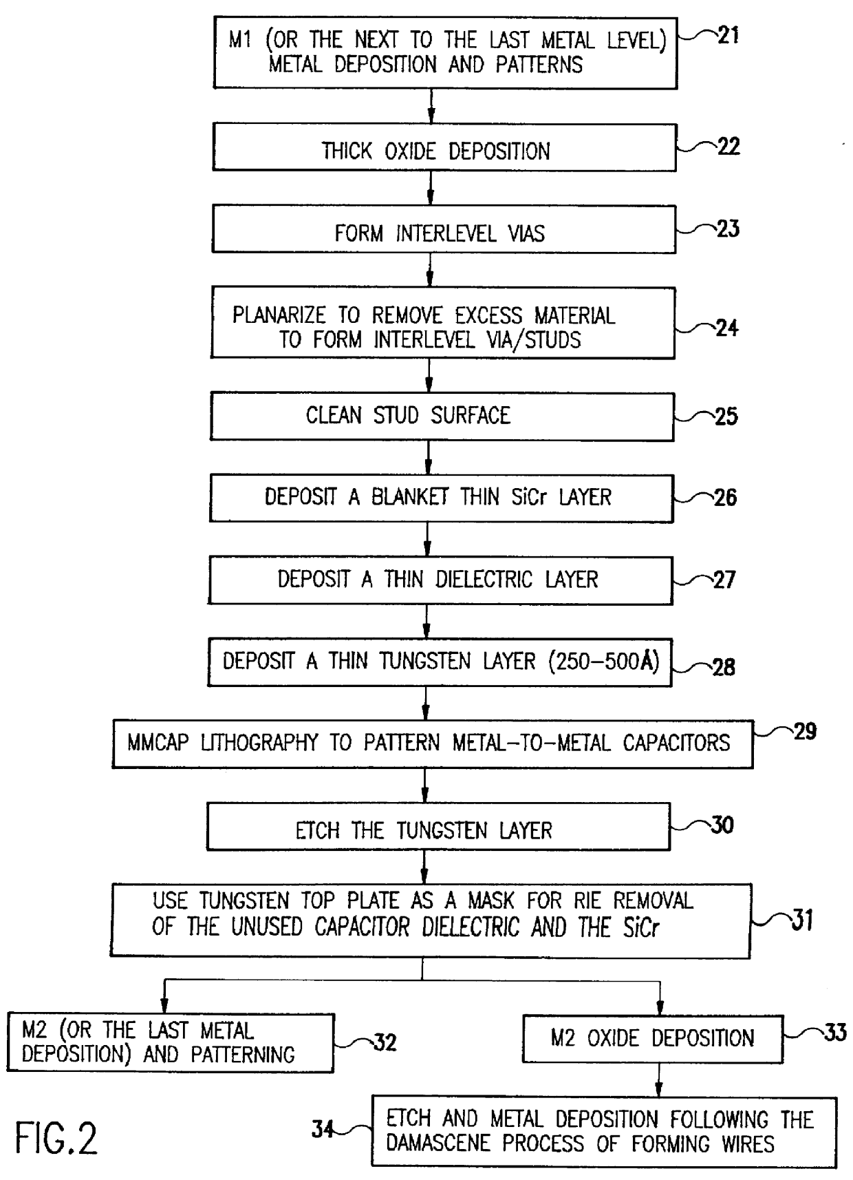
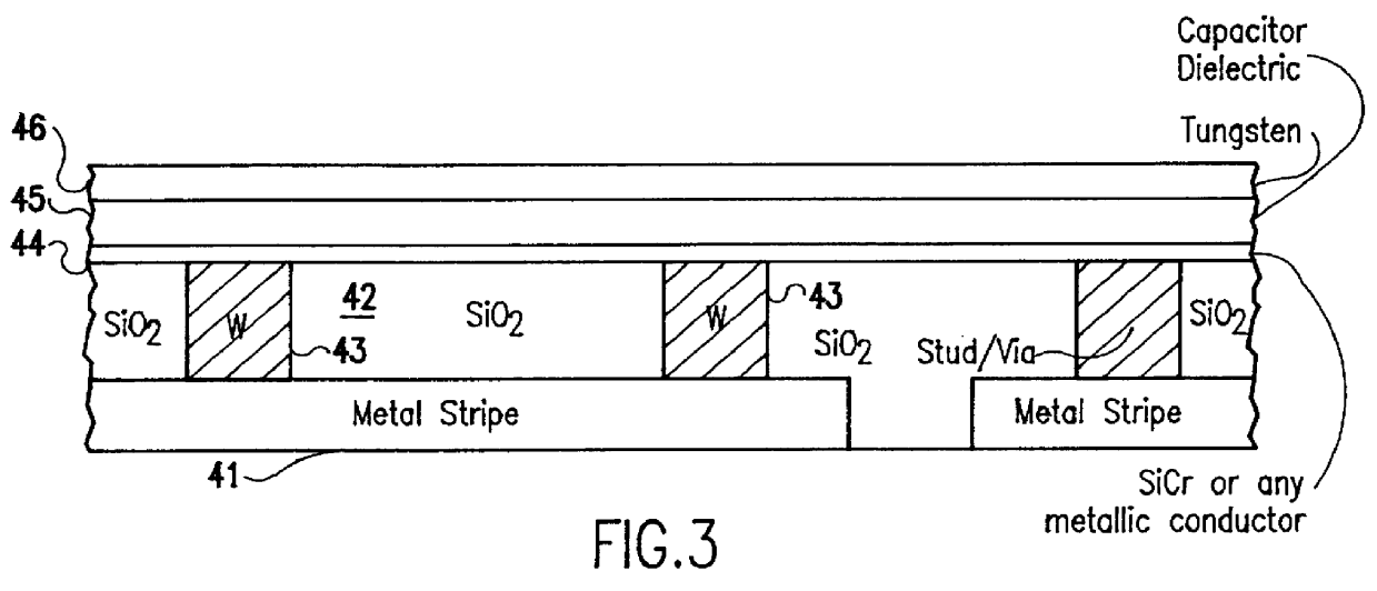
Referring again to the drawings, and more particularly to FIGS. 2 and 3, there is shown in FIG. 2 a flow diagram of the method of producing a metal-to-metal capacitor (MMCAP) for use in integrated circuit applications such as decoupling capacitors. In function block 21, the first metallization layer (M1), or the next to the last metal level, is deposited and patterned. This metal layer is layer 41 in FIG. 3. Thick oxide deposition is done in function block 22 for interlevel insulation. The thick oxide 42, here SiO.sub.2, is deposited over the metal layer 41. Next, interlevel vias are formed in function block 23 and then filled using any desired materials (e.g., AlCu, W, Cu, Al, AlCuSi, etc.) to form studs to contact underlying polycrystalline silicon or diffusions formed in the integrated circuit. In FIG. 3, the studs 43 are formed of W. A planarization process is used in function block 24 to remove excess material to form the interlevel studs. The stud surface is cleaned in functio...


PUM


Abstract

A method of fabricating on chip metal-to-metal capacitors (MMCAP) uses planar processing with a flexible choice of dielectric, thickness and capacitor shape. The method provides a simpler process which has a better yield and more reliable structure by creating a metal-to-metal capacitor on a planar surface, not in deep trenches. In addition to the process simplicity, the method also allows the use of any dielectric materials which are needed by the product designer; e.g., higher or lower dielectric constant and also not limited by high etch rate difference. Because the inventive process is a planar process, there are no corners in the bottom of deep trenches to cause yield and reliability problems. The capacitor area can be adjusted to any shape because there are no edge effects.

Description

1. Field of the InventionThe present invention generally relates to the manufacture of electrical capacitors for use in integrated circuits and, more particularly, to a method of fabricating on chip metal to metal capacitors using planar processing techniques for applications such as on-chip decoupling capacitors.2. Background DescriptionPresently, decoupling capacitors on an integrated circuit chip are fabricated by adding a thin dielectric layer between two metal layers as follows. First, with reference to FIG. 1, a lower metal (M1) 11 is deposited on an oxide layer 12 and patterned. After the M1 11 is deposited and patterned, a thick interlevel dielectric (ILD) 13 is applied. The ILD is then etched for both contact vias 14 and for the region 15 where the capacitor is to be formed. A blanket thin dielectric (TD) 16 is then deposited. Conventional photolithographic techniques are used to remove the TD from the contact via holes. In the structure shown, a tungsten stud 17 is formed ...

Claims


Application Information

Patent Timeline
Patent Type & Authority Patents(United States)
IPC IPC(8): H01L21/02H01L21/768H01L21/70
CPCH01L21/76838H01L28/40Y10S438/945H01L28/60
Inventor NGUYEN, DU B.RATHORE, HAZARA S.PROKOP, GEORGE S.WACHNIK, RICHARD A.GRUSZECKI, CRAIG R.
Owner GLOBALFOUNDRIES INC
Why Eureka
Try Eureka