Method of producing an anodic bonded semiconductor sensor element

a technology of anodic bonding and semiconductor sensor element, which is applied in the direction of semiconductor devices, instruments, measurement devices, etc., can solve the problems of unexpected breakage of semiconductor sensor elements and occurrence of electric discharge at a sufficiently high reliability

Inactive Publication Date: 2000-06-20
DENSO CORP +1
View PDF17 Cites 25 Cited by
  • Summary
  • Abstract
  • Description
  • Claims
  • Application Information

AI Technical Summary

Problems solved by technology

However, the present inventors found that the above-described conventional mount often induced unexpected breakage of the semiconductor sensor element when such sensors were actually made and used.
Therefore, the amount of the

Method used


Image

  • Method of producing an anodic bonded semiconductor sensor element
  • Method of producing an anodic bonded semiconductor sensor element
  • Method of producing an anodic bonded semiconductor sensor element

Examples


first embodiment

A semiconductor sensor mount of a first embodiment will now be described in detail with a manufacturing method therefor.

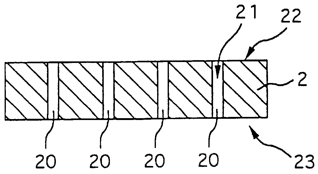
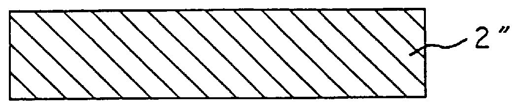
The manufacturing method of the semiconductor sensor mount according to the first embodiment employs as a base material a glass plate 2" made of an aluminosilicate glass plate 3.0 mm thick cut to the prescribed size, as illustrated in FIG. 1A.

The aluminosilicate glass used was composed mainly of 60 wt. % of silicon oxide, 15 wt. % of alumina, 10 wt. % of zinc oxide, some percentage of boron oxide, magnesium oxide and sodium oxide, respectively, and 1 wt. % of other substances. The characteristics of each type of aluminosilicate glass, such as the composition and the coefficient of thermal expansion, are described in detail in the Japanese Unexamined Patent Publication No. 4-83733 entitled "Glass for Silicon Pedestal."

Firstly, as illustrated in FIG. 1B, in the glass plate 2" cut as illustrated in FIG. 1A are formed, by means of ultrasonic honing, a plurality of thro...

second embodiment

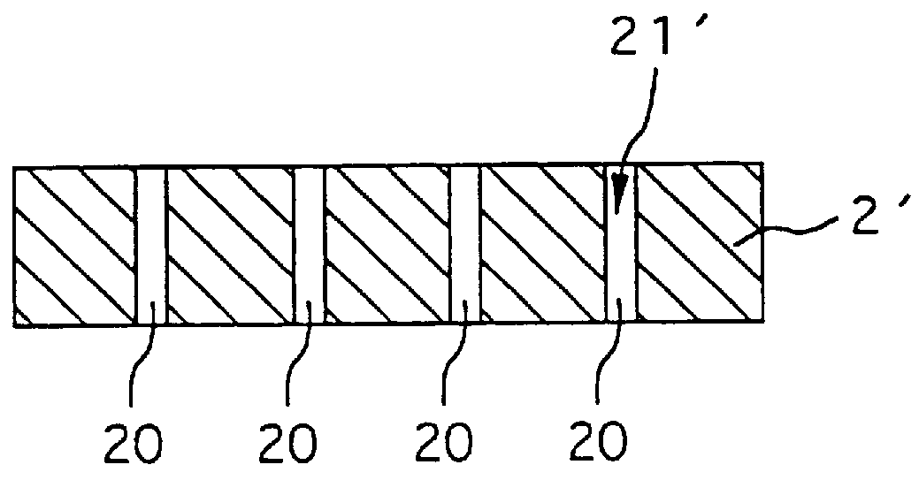
In a semiconductor sensor mount and the manufacturing method therefor according to a second embodiment, the flat plate as a material plate of the mount has a two-layer structure as illustrated in FIG. 7. That is, the flat plate is a hole-provided flat plate 2D constructed in two layers; one is a thin glass layer 2G, and the other is a silicon layer 2S anodically bonded to one side of the thin glass layer 2G in a previous process.

The glass layer 2G is made of an aluminosilicate glass plate of 0.15 mm thick, in which the side opposite to the silicon layer 2S has been mirror polished and forms the anodic bonding surface 22. On the other hand, the silicon layer 2S is a wafer made of a silicon monocrystal of 2.0 mm thick. Accordingly, the total plate thickness of the hole-provided flat plate 2D is 2.15 mm.

In the hole-provided flat plate 2D are checkeredly arranged a plurality of through holes 20 formed by the ultrasonic honing method in the same way as the first embodiment. By etching th...


PUM


Abstract

A semiconductor sensor mount is formed as follows: through holes are formed that penetrate a glass plate; and then the glass plate having the through holes is dipped into hydrofluoric acid etchant to smooth the inner peripheral surfaces of the respective through holes. By etching the inner peripheral surfaces of the respective through holes after the through hole formation, minute roughness and cracks formed on the inner peripheral surfaces are removed, and thereby the areas for adsorbing gas are substantially reduced. That is, vacuums within the through holes can be maintained at a high degree during the anodic bonding, whereby undesirable electric discharge phenomena are prevented even if a relatively high voltage is applied during the anodic bonding. Accordingly, the yield of products can be improved while improving productivity.

Description

This application is based upon and claims the benefit from priority of the prior Japanese Patent Application No. 7-164169 filed on Jun. 29, 1995, the contents of which are incorporated herein by reference.1. Field of the InventionThe present invention generally relates to a semiconductor element mount to which a semiconductor element is anodically bonded. The mount according to the present invention is applicable to a semiconductor sensor for measuring pressure, acceleration, etc., for example, in which a semiconductor sensor element is anodically bonded to the mount.2. Related ArtsSome conventional semiconductor sensors for measuring pressure are provided with a glass-made mount which is to be anodically bonded to a semiconductor sensor element. In such a mount, a through hole opens to the anodically bonded surface and communicates with a diaphragm of the semiconductor sensor element.A technique has been developed by which thermal stress can be eased by utilizing a mount made of a ...

Claims


Application Information

Patent Timeline
IPC IPC(8): G01L9/00H01L29/84G01L9/04H01L21/302H01L21/3065H01L21/308
CPCG01L9/0042
Inventor FUKADA, TSUYOSHISUZUKI, YASUTOSHISATOH, KOUSHUKAWASHIMA, HIROAKI
Owner DENSO CORP
Why Eureka
Try Eureka