Plasma processing apparatus

a processing apparatus and plasma technology, applied in the direction of chemical vapor deposition coating, coating, electric discharge tube, etc., can solve the problems of reducing the rf energy to be supplied to the process room, reducing the coefficient of use of an applied energy from an rf power supply, etc., to achieve accurate control of the progress of dissociation of process gas, increase the coefficient of use of an applied energy, and high density

Inactive Publication Date: 2000-07-18
TOKYO ELECTRON LTD +1
View PDF5 Cites 96 Cited by
  • Summary
  • Abstract
  • Description
  • Claims
  • Application Information

AI Technical Summary

Benefits of technology

Therefore, it is an object of the present invention to provide a plasma processing apparatus of the RF induction coupling type, which can increase the coefficient of use of an applied energy from an RF power supply, and generate uniform plasma of a high density even under a low pressure condition.
It is another object of the present invention to provide a plasma processing apparatus of the RF induction coupling type having a shower head, which can uniformly turn a process gas into plasma, thereby accurately controlling the progress of dissociation of the process gas.

Problems solved by technology

As a result, a problem arises such that the coefficient of use of an applied energy from an RF power supply is decreased.
This problem becomes prominent in a plasma processing apparatus having a big size for processing a wafer of a large diameter or an LCD substrate of a large surface area.
As a result, part of an RF energy supplied from the antenna is consumed by generating plasma in the distribution room, thereby decreasing the RF energy to be supplied to the process room.

Method used


Image

  • Plasma processing apparatus
  • Plasma processing apparatus
  • Plasma processing apparatus

Examples


Embodiment Construction

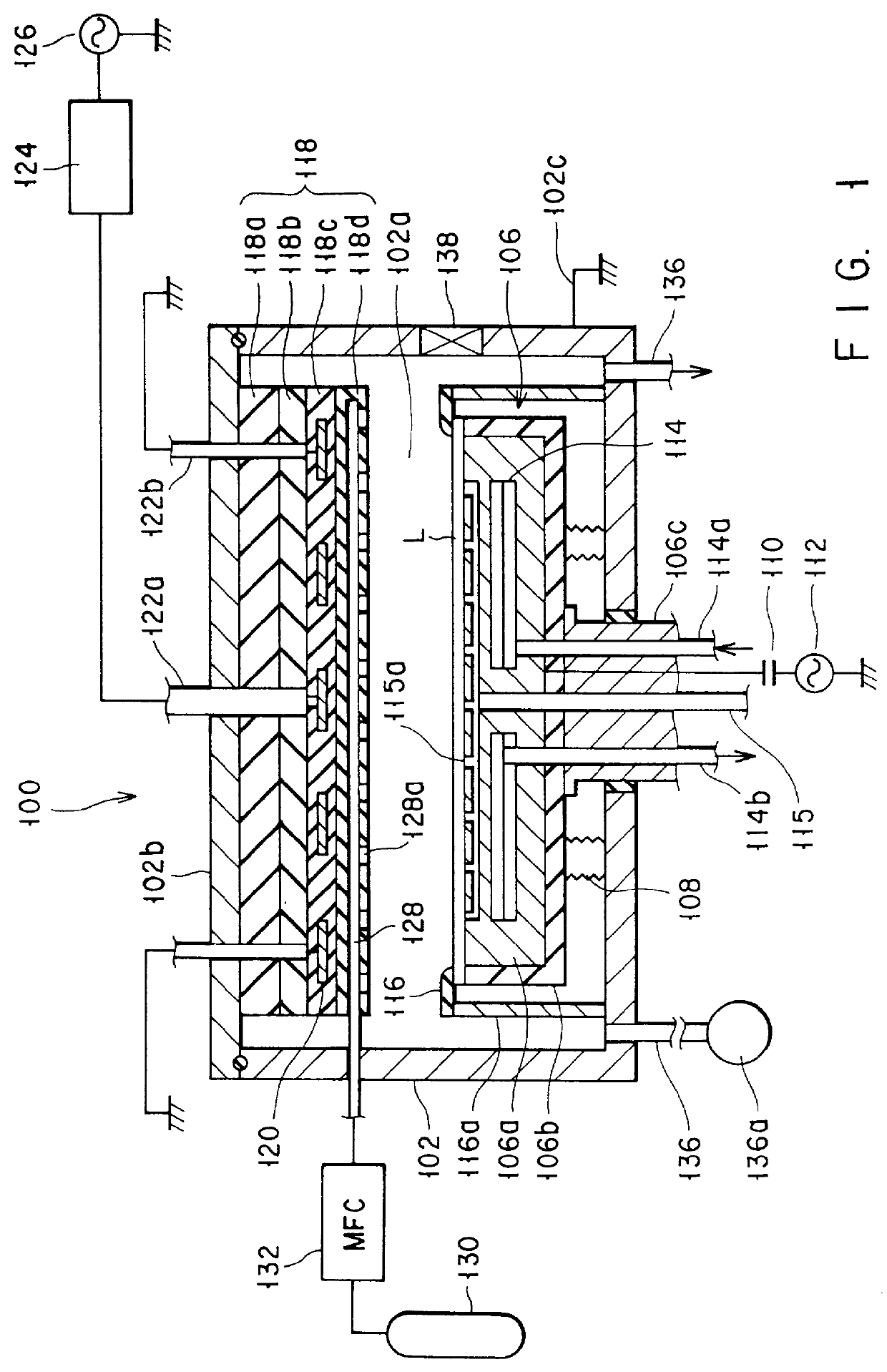
FIG. 1 is a cross-sectional view showing an etching apparatus of an LCD substrate, which is an application of a plasma processing apparatus according to an embodiment of the present invention.

The plasma etching apparatus 100 shown in FIG. 1 has a process container 102 which is made of a conductive material, such as aluminum having an oxidized alumite surface or stainless steel, and has a cylindrical or rectangular box shape. A predetermined etching process is performed in a process room 102a formed in the process container 102.

The process container 102 is grounded through a line 102c. A work table 106 having an essentially rectangular shape is arranged on the bottom of the process container 102 for mounting a target object, such as an LCD substrate L. The work table 106 is constituted by an electrode portion 106a made of a conductive material, such as aluminum having an oxidized alumite surface or stainless steel, and an electrode protecting portion 106b made of an insulating materi...


PUM

PropertyMeasurementUnit
frequencyaaaaaaaaaa
pressureaaaaaaaaaa
atmospheric pressureaaaaaaaaaa

Abstract

A plasma etching apparatus of the induction coupling type for processing an LCD substrate has a process container forming an airtight process room. A work table is arranged in the process room for supporting the LCD substrate. A vacuum pump is arranged for exhausting and setting the process room into a vacuum state. An antenna block having a plurality of dielectric layers is arranged to face the work table. An RF antenna is embedded in one of the dielectric layers of the antenna block for forming an electric field. A power supply is connected to the RF antenna for applying an RF power. The lowermost layer of the antenna block is formed as a shower head for supplying a process gas into the process room from a position between the RF antenna and the work table. At least part of the process gas is turned into plasma by the electric field. In the layer formed as the shower head, the gas passage has such a projected area ratio, on a planar outer-contour of the mount surface of the work table, that is from 15% to 25%.

Description

BACKGROUND OF THE INVENTIONThe present invention relates to a plasma processing apparatus, and particularly to a plasma processing apparatus of the induction coupling type in which induction plasma is excited in a process room by applying an RF (radio frequency) power to an RF antenna.In recent years, with an increase in the degree of integration level of a semiconductor device and an LCD (liquid crystal display), it has become necessary to perform an ultra fine process of the order of sub-micron and furthermore of sub-half-micron. In order to perform such a process in a plasma processing apparatus, it is important to control high density plasma with high accuracy under a low pressure atmosphere, such as between 1 mTorr and 50 mTorr. It is also necessary to form the plasma to have a high uniformity and a large area so as to correspond to a wafer of a large diameter or an LCD substrate of a large size.In consideration of these technical demands, a lot of approaches have been made to ...

Claims


Application Information

Patent Timeline
Patent Type & Authority Patents(United States)
IPC IPC(8): C23C16/00
CPCC23C16/00H01J37/3244H01J37/321H01J37/32082
Inventor HAMA, KIICHI
Owner TOKYO ELECTRON LTD
Why Eureka
Try Eureka