

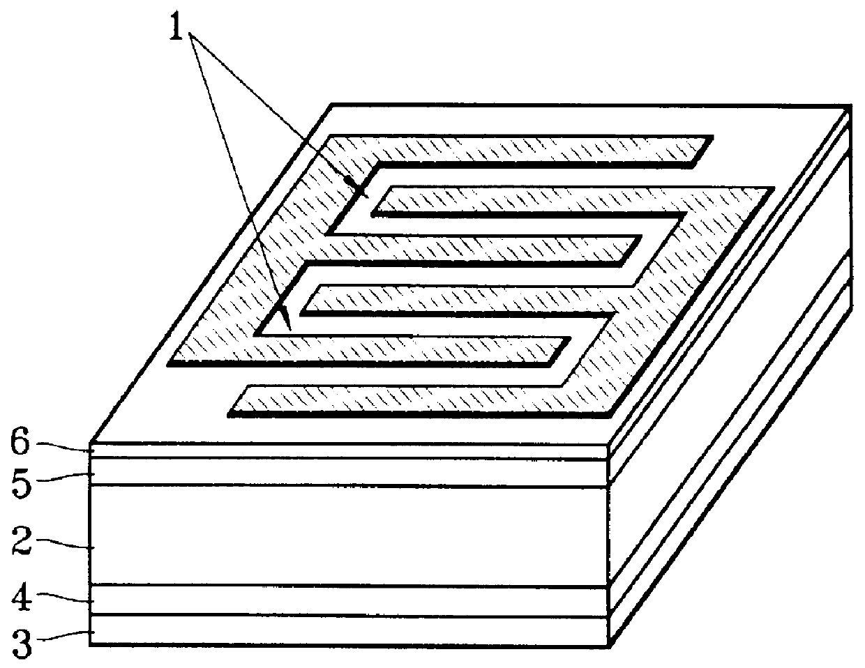
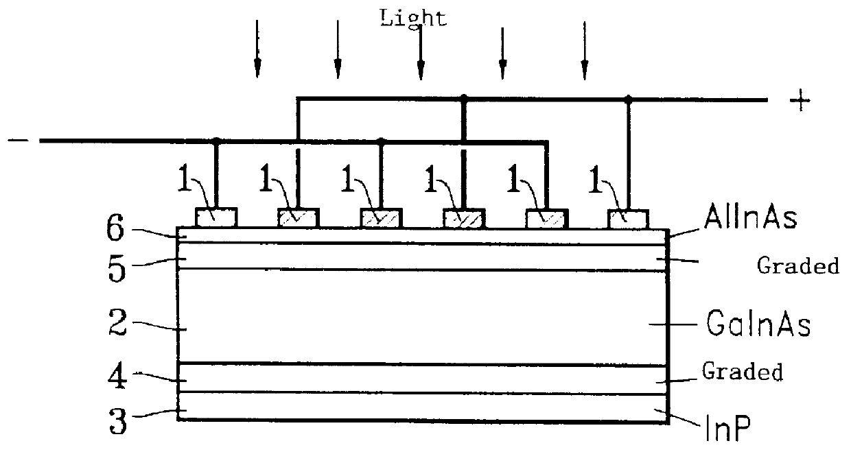
Metal-semiconductor-metal photodetector
a metal-semiconductor and photodetector technology, applied in the field of photodiodes, can solve the problems of affecting the overall performance of the detector, and affecting the overall speed of the devi
- Summary
- Abstract
- Description
- Claims
- Application Information
AI Technical Summary
Benefits of technology
Problems solved by technology
Method used
Image

Examples
Embodiment Construction
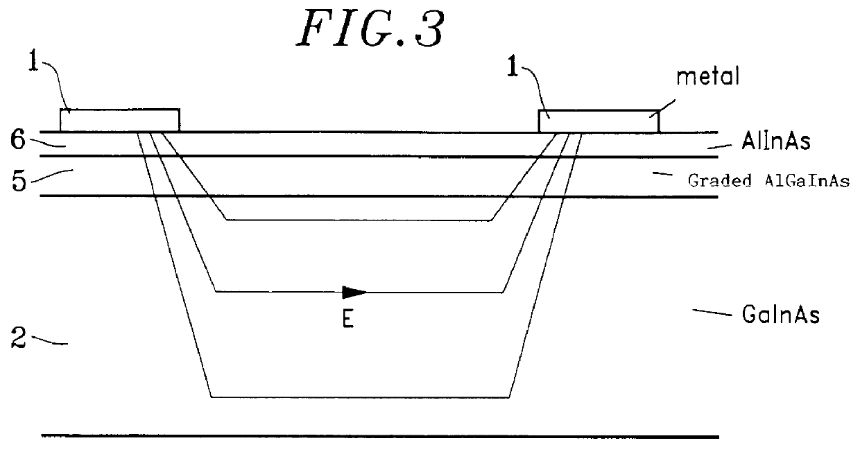
In FIG. 4, only that portion which corresponds to the positively biased electrode is shown.
The energy levels of the conduction band CB and of the valence band VB shown in dashed lines in FIG. 4 corresponds to those of the structure of FIGS. 1 to 3; the levels shown in continuous lines correspond to the same structure in which a doping plane 7 has been added between the absorbent layer 2 and the graded transition layer.
In FIG. 4, it can be observed that including the doping plane 7 makes it possible to eliminate the potential barrier in the conduction band, thereby improving operation at moderate bias voltages (better collection at low illumination, which should lead to digital transmission via an improved reception threshold).
The energy levels in FIG. 4 correspond to n-type residual doping in the vicinity of 10.sup.15 / cm.sup.3.
It is important to determine accurately the charge of the doping plane 7 so as to avoid a situation in which holes are trapped in the vicinity of the negativ...
PUM
 Abstract
Description
Claims
Application Information