
Atomically sharp field emission cathodes
a field emission cathode and atomically sharp technology, applied in the field of atomically sharp field emission cathodes, can solve the problems of poor uniformity in the curvature radius of the tips, and achieve the effects of smooth surface morphology, improved uniformity, and improved sharpness of the tips
- Summary
- Abstract
- Description
- Claims
- Application Information
AI Technical Summary
Benefits of technology
Problems solved by technology
Method used
Image

Examples
Embodiment Construction
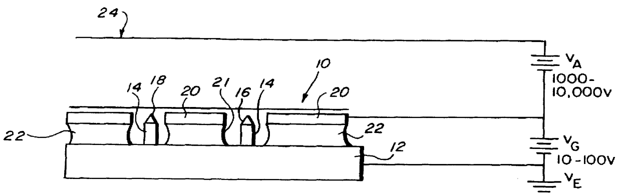
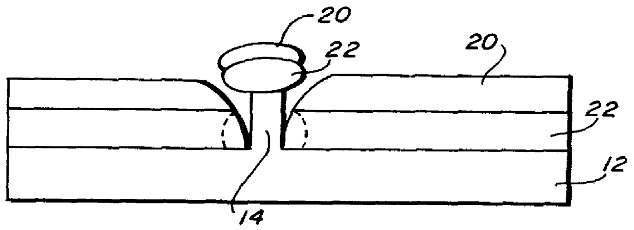
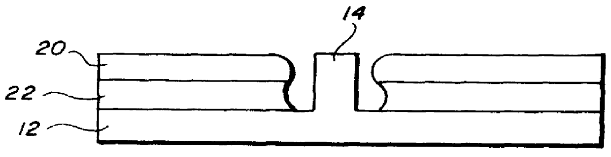
The field emitter array of this invention includes a plurality of semiconducting nanomesas disposed on a semiconducting substrate, microscopic three-dimensional monocrystalline emitting regions or tips on the nanomesas of a semiconducting material each terminating in an apex; and a gate around the nanomesas to provide an extraction bias voltage for field emission such that the emitted electrons travel from the apexes of the tips to the anode when the field emitter is in operation. The gate is supported by a dielectric material disposed on the substrate. The fabrication process generally includes lithography and etching to form nanomesas disposed on a substrate, gate fabrication by directional or conformal deposition and etching, and tip formation by epitaxial self-assembly of semiconducting material deposited on the nanomesas which tips terminate in atomically sharp apexes.
The unique physical property of self-assembly by vapor phase epitaxial growth is used to create atomically shar...
PUM
 Abstract
Description
Claims
Application Information