Low-power column parallel ADC in CMOS image sensors

a low-power column and cmos image technology, applied in the field of low-power column parallel adc in cmos image sensors, can solve the problems of large power dissipation, large power consumption, and many wasted power, and achieve the effect of reducing the number of switching, and reducing the power consumption

Inactive Publication Date: 2000-10-24
HANGER SOLUTIONS LLC
View PDF4 Cites 57 Cited by
  • Summary
  • Abstract
  • Description
  • Claims
  • Application Information

AI Technical Summary

Benefits of technology

Invention resides in a new low-power column parallel ADC architecture for image sensors which reduces the power consumption by reducing the number of switchings of a comparator to digitize a row of pixel data. Two ramp reference signals are provided in accordance with the principles of this invention. A first ramp signal is provided to each comparator that is clocked with an associated first clock signal. Each column comparator compares the first ramp signal to the pixel data using the first clock, wherein the first clock (clock1) corresponds to N multiple of a second clock signal (clock2), with N>1. Only when the column comparator detects a first crossover with the first ramp signal, then clock2 is provided to clock each comparator and to detect a second crossover point with the second reference signal. This arrangement can greatly reduce the number of switchings required to digitize a row of pixel data, thereby also providing significant power saving.

Problems solved by technology

Conventional ADCs, however, suffers a shortcoming of causing large power dissipation.
A row of ADC comparators is continuously switching at every clock cycle resulting in significant power consumption, particularly when the number of comparators needed increases with the size of the image sensors, with some large format sensors now requiring greater than a thousand comparators.
Moreover, the continuous switchings of the comparators result in much wasted power since only switchings around the crossover point are particularly relevant.

Method used


Image

  • Low-power column parallel ADC in CMOS image sensors
  • Low-power column parallel ADC in CMOS image sensors
  • Low-power column parallel ADC in CMOS image sensors

Examples


Embodiment Construction

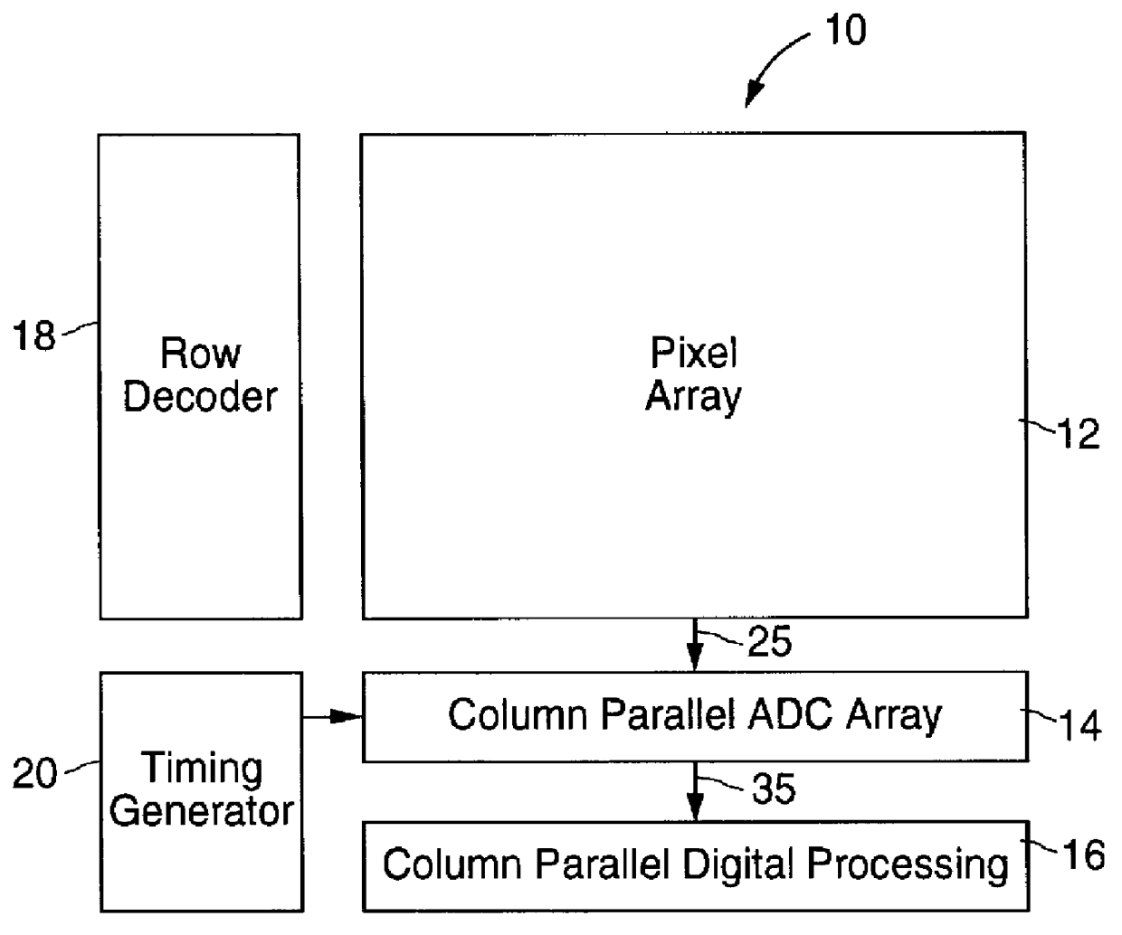
FIG. 1 is a general system-level block diagram of a low-power column parallel ADC image sensor architecture designed in accordance with the principles of this invention. Low-power column parallel ADC image sensors architecture 10 reduces power consumption by reducing the number of switching operations of an array of comparators 14 necessary to digitize a row of pixel data from pixel array 12.

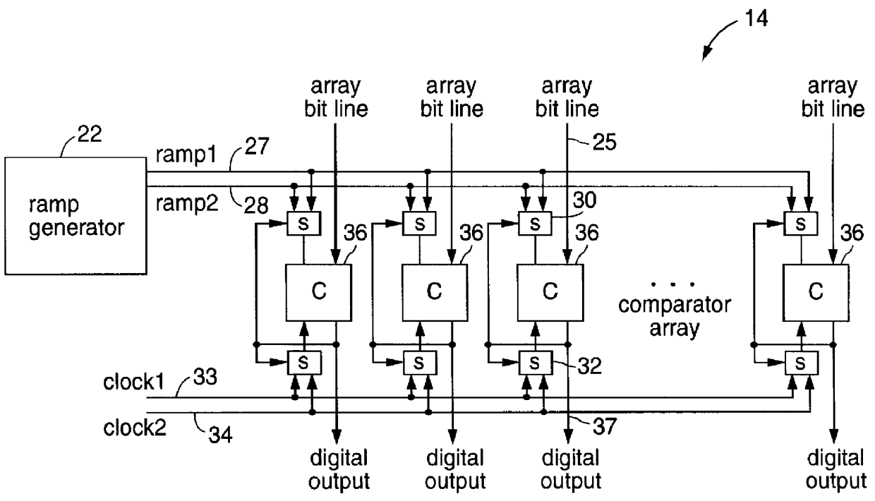
FIG. 2 provides a more detailed logic block diagram of the low-power column parallel ADC array of FIG. 1. Two ramp reference signals 27 and 28 provided by a ramp generator 22 in timing generator 20 (FIG. 1) are provided as input to column parallel ADC array 14. A first ramp signal (ramp1) 27 and a second ramp signal (ramp2) 28 are provided to each comparator 36 of array 14 via a first multiplexer 30. In each column comparator 36, first ramp signal 27 is compared to an input array bit line signal 25 using a first clock signal (clock1) 33 from timing generator 20 provided as input clock to each co...


PUM


Abstract

A low-power column parallel ADC architecture for image sensors that reduces the power consumption by reducing the number of switchings of a comparator to digitize a row of pixel data. Two ramp reference signals are provided in accordance with the principles of this invention. A first ramp signal is provided to each comparator that is clocked with an associated first clock signal. In each column comparator, the first ramp signal is compared to the pixel data using clock1, wherein clock1 corresponds to N multiple of a second clock signal (clock2), with N>1. Only when the column comparator detects a first crossover with the first ramp signal, then the comparator switches at every clock cycle of the second clock, clock2, to compare and detect a second crossover point with the second reference signal. This arrangement can greatly reduce the number of switchings required to digitize a row of pixel data, thereby resulting in significant power saving.

Description

The invention relates generally to analog-to-digital converters (ADCs), and more particularly to ADCs in CMOS image sensors.BACKGROUND OF INVENTIONConventional CMOS imager sensors read out a row of pixel values at a time to increase the read-out bandwidth, with a row of pixel values digitized in parallel by means of an ADC provided for each pixel column. Such conventional imaging sensor ADCs are illustrated in U.S. Pat. No. 4,851,839 to Reinke, U.S. Pat. No. 5,613,156 to Katayama, and U.S. Pat. No. 5,461,425 to Fowler, et al. Typically, these ADCs comprise a comparator with one of the comparator inputs connected to the bit line of the pixel and the other input connected to a reference signal that is a ramp signal. At every clock cycle, the bit line of the pixel is compared to the reference signal. Initially, the reference signal is less than the pixel signal (e.g., the bit line value), and thus the comparator generates a "0" output value. When the ramp reference crosses the pixel si...

Claims


Application Information

Patent Timeline
Patent Type & Authority Patents(United States)
IPC IPC(8): H03M1/00H03M1/50H03M1/56H03M1/12H04N5/335
CPCH03M1/002H04N5/335H03M1/56H03M1/123H04N25/00
Inventor XIAO, PETER HONG
Owner HANGER SOLUTIONS LLC
Why Eureka
Try Eureka