Method for forming barrier layer for copper metallization

a technology of barrier layer and copper metallization, which is applied in the direction of semiconductor devices, semiconductor/solid-state device details, electrical devices, etc., can solve the problems of difficult to achieve ion etching, many difficulties that must be overcome with respect to the process, and difficult to form copper wiring patterns

Inactive Publication Date: 2000-11-21
TOSHIBA MEMORY CORP
View PDF5 Cites 57 Cited by
  • Summary
  • Abstract
  • Description
  • Claims
  • Application Information

AI Technical Summary

Problems solved by technology

However, in realizing copper wirings, there are many difficulties that must be overcome with respect to the process for forming them.
Essential problems with the process of forming copper wirings are as follows: The first is that copper RIE (reactive ion etching) is difficult to attain and therefore copper wiring patterns are difficult to form.
The second is that copper diffuses through interlayer insulating films (silicon oxide films) due to heat and electric field, thereby often having some negative influences on the other devices in LSI and causing electric leak through wirings therein.
Since the oxide film is thick and its mechanical and chemical strength is low, it interferes with the formation of good copper wirings.
However, the first method is problematic in that the capacitance between the wirings is increased due to the SiN film 61 formed on the interlayer insulating film 12 around the copper wiring 14 and having a high dielectric constant, thereby lowering the acting speed of LSI.
The second method is problematic in that the selective formation of the barrier layer is difficult to control and therefore the short-circuit margin between the wirings is low, and that a chlori

Method used


Image

  • Method for forming barrier layer for copper metallization
  • Method for forming barrier layer for copper metallization
  • Method for forming barrier layer for copper metallization

Examples


first embodiment

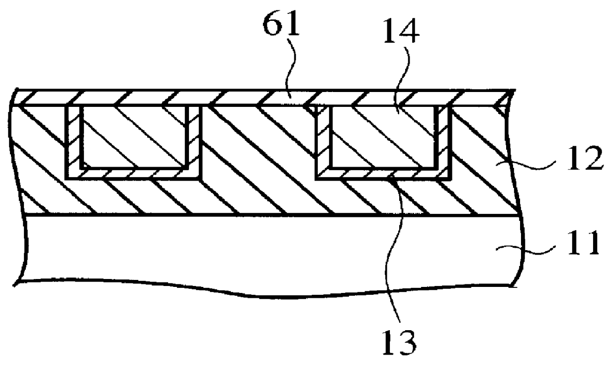
Referring now to FIGS. 5A to 5C, the present invention is described.

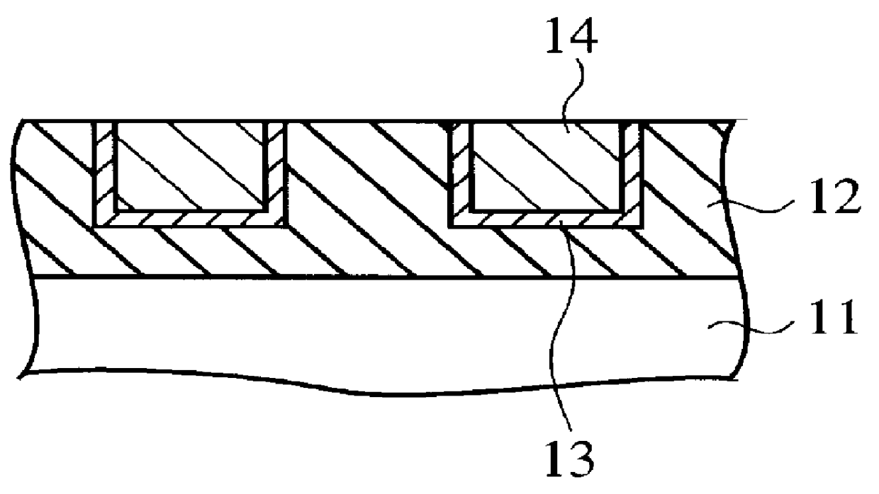
Wiring grooves are first formed in the surface of an interlayer insulating film 12,such as a silicon oxide film,as formed on a semiconductor substrate 11,such as a silicon substrate. Though not shown, semiconductor chips such as transistors and others are formed on the silicon substrate 11. Next, a TiN film (titanium nitride film) 13, which is to be a barrier metal layer for the bottom and the side surface of the copper wiring to be formed, is formed on the entire surface through chemical sputtering, and thereafter copper wiring 14 is formed through electrolytic plating. Next, all the TiN film 13 and the copper film 14 except those in the grooves are entirely removed through CMP (chemical mechanical polishing). Thus is formed the embedded copper wiring (FIG. 5A).

The substrate thus having the copper wiring 14 formed thereon is introduced into a closed container, which is filled with a monosilane ambient under a press...

second embodiment

the present invention is described with reference to FIGS. 6A to 6D, in which the same or corresponding constituent elements as or to those in the first embodiment illustrated in FIGS. 5A to 5C are referred to by way of the same numeral references as in FIGS. 5A to 5C.

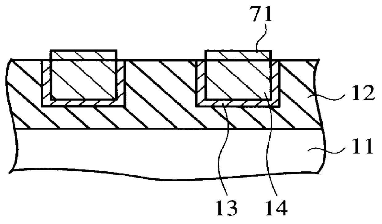
The steps of FIG. 6A and FIG. 6B are the same as those in FIG. 5A and FIG. 5B for the first embodiment.Briefly, copper wiring 14 is formed via a TiN film 13 to be a barrier metal layer, in the wiring grooves formed in an interlayer insulating film 12 (FIG. 6A), and thereafter a silicon film 15 is selectively formed on the surface of the copper wiring 14 through heat treatment with a monosilane (FIG. 6B).

Next, the substrate thus having the silicon film 15 formed on the surface of the copper wiring 14 is transported into a sputtering chamber preferably without breaking the vacuum atmosphere around it. In the chamber, Ti is sputtered onto it through magnetron sputtering, for which the target is Ti, the pressure is 3 Pa, t...

third embodiment

the present invention is described with reference to FIGS. 7A to 7E, in which the same or corresponding constituent elements as or to those in the first embodiment illustrated in FIGS. 5A to 5C are referred to by way of the same numeral references as in FIGS. 5A to 5C.

The steps of FIG. 7A and FIG. 7B are the same as those in FIG. 5A and FIG. 5B for the first embodiment. Briefly, copper wiring 14 is formed via a TiN film 13 to be a barrier metal layer, in the wiring grooves formed in an interlayer insulating film 12 (FIG. 7A), and thereafter a silicon film 15 is selectively formed on the surface of the copper wiring 14 through heat treatment with a monosilane (FIG. 7B).

Next, the substrate thus having the silicon film 15 formed on the surface of the copper wiring 14 is transported into a sputtering chamber preferably without breaking the vacuum atmosphere around it. In the chamber, Ni is sputtered onto it through magnetron sputtering, for which the target is Ni, the pressure is 3 Pa, ...


PUM


Abstract

A method comprises forming a barrier layer for copper metallization, selectively forming a silicon film on a surface of copper wiring formed on the main surface of a semiconductor substrate, and reacting the silicon film with a non-copper metal and/or nitrogen to form a barrier layer in a self-aligned manner relative to the copper wiring. In the method, the capacitance increase in the copper wirings formed is prevented, and the barrier layer formed has a satisfactory barrier property of protecting the copper wirings.

Description

1. Field of the InventionThe present invention relates to the field of semiconductor manufacturing techniques for copper metallization , and in particular, to a method for forming barrier layer for copper metallization.2. Description of the Prior ArtHeretofore, in general, aluminum wirings have been being used in LSI. Copper wirings are being developed in the art as low-resistance metal wirings having higher electric conductivity and reliability over Al wirings. The specific resistivity of copper is around 1.8 .mu..OMEGA..multidot.cm or so, while that of aluminum is around 2.9 .mu..OMEGA..multidot.cm or so, and it is expected that copper wirings will bring about the reduction in electric resistance of around 40% or so, when compared with aluminum wirings.However, in realizing copper wirings, there are many difficulties that must be overcome with respect to the process for forming them. Still now, therefore, aluminum is the mainstream of the wiring material for LSI from the birth of ...

Claims


Application Information

Patent Timeline
IPC IPC(8): H01L21/768H01L21/70H01L21/3205H01L21/28H01L23/52
CPCH01L21/76834H01L21/76855H01L21/76849H01L21/76846
Inventor MATSUDA, TETSUOIIJIMA, TADASHIKANEKO, HISASHI
Owner TOSHIBA MEMORY CORP
Why Eureka
Try Eureka