Semiconductor integrated circuit device

a technology of integrated circuits and semiconductors, applied in the direction of memory adressing/allocation/relocation, digital storage, instruments, etc., can solve the problems of large number of external pin terminals compared with the number of a single dram, delay in data transfer operation, and insufficient dram operation speed

Inactive Publication Date: 2000-11-21
RENESAS ELECTRONICS CORP
View PDF18 Cites 16 Cited by
  • Summary
  • Abstract
  • Description
  • Claims
  • Application Information

AI Technical Summary

Problems solved by technology

However, the operating speed of the DRAM is still insufficient and, in order to solve this problem, it is usual to provide a sub-memory between the MPU and the main memory.
These prior arts have problems such as delay of data transfer operation in a case of cache mishit and techniques which solve such problem has been proposed.
However, there are the following problems in the above mentioned CDRAM.
First, since address pin terminals and control pin terminals are provided separately for the DRAM array and the SRAM array, the number of external pin terminals is very large compared with that of a single DRAM.
Therefore, there is no compatibility of a substrate, etc., on which the semiconductor memory is mounted, with respect to that of a usual DRAM, etc.
Second, in the bi-directional transfer gate circuit, the number of circuits each havi

Method used


Image

  • Semiconductor integrated circuit device
  • Semiconductor integrated circuit device
  • Semiconductor integrated circuit device

Examples


Embodiment Construction

of the Respective Blocks

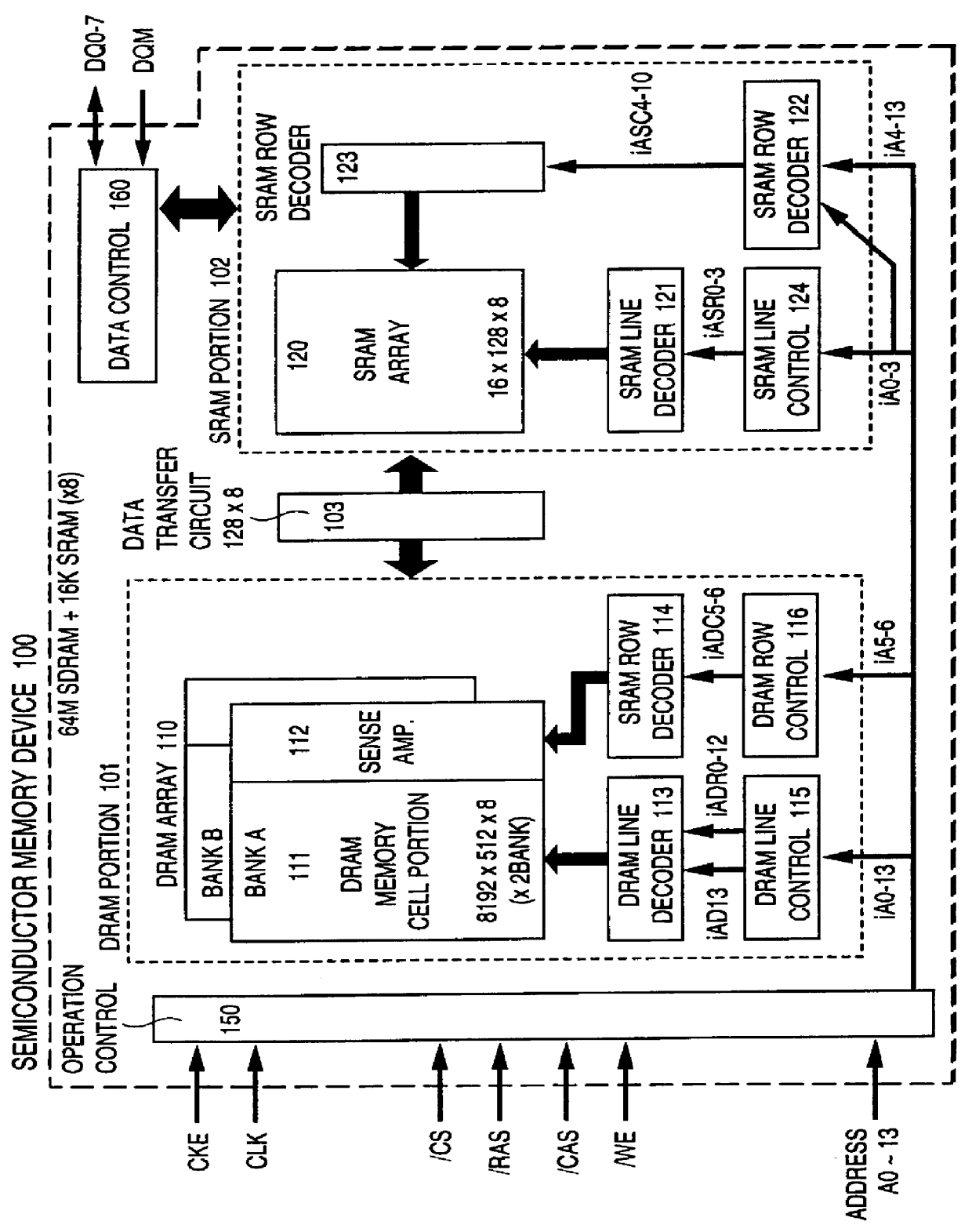
The respective circuit blocks of the overall block diagram shown in FIG. 1 will be described in detail. It should be noted that the following description is for a mere embodiment and this invention is not limited thereto.

1. {Operation Control Circuit}

FIG. 54 is a circuit diagram of the operation control circuit 150.

The operation control circuit 150 is constructed with an internal clock generator circuit 410, a command decoder 420, a control logic 430, an address control circuit 440 and a mode register 450.

The internal clock generator circuit 410 generates an internal clock signal iCLK from the external input signals CLK and CKE.

The internal clock signal ICLK is supplied to the command decoder 420, the control logic 430, the address control circuit 440 and the data control circuit to control the timing of the respective portions.

The command decoder 420 includes a buffer 421 for receiving the respective input signals and a command judge circuit 422. The / CS sig...


PUM


Abstract

A semiconductor integrated circuit device includes a main memory portion and a sub memory portion including a plurality of memory cell groups, wherein a bi-directional data transfer is performed between an arbitrary area of the main memory portion and each of the plurality of the memory cell groups and the plurality of the memory cell groups function as independent cache memories, respectively. Therefore, the semiconductor integrated circuit device of the present invention has a main memory suitable for being accessed from a plurality of data processors.

Description

1. Field of the InventionThe present invention relates to a semiconductor integrated circuit device and, particularly, to a semiconductor integrated circuit device having a main memory portion and a sub-memory portion formed in a semiconductor substrate and a data transfer circuit provided between the main memory portion and the sub-memory portion.2. Description of the Related ArtIn general, a relatively low speed, inexpensive semiconductor device having large memory capacity, such as general purpose DRAM, is used as a main memory in a computer system.In a recent computer system, an operating speed of a DRAM constituting a main memory is increased with increase of an operating speed of the system, particularly, of a MPU thereof. However, the operating speed of the DRAM is still insufficient and, in order to solve this problem, it is usual to provide a sub-memory between the MPU and the main memory. Such sub-memory is generally called as a cache memory and is constructed with a high ...

Claims


Application Information

Patent Timeline
IPC IPC(8): G11C7/10G11C11/00G06F12/08G11C11/41G11C11/401
CPCG11C7/103G11C7/1045G11C11/005G11C7/1075G11C7/1072G11C7/00
Inventor MAESAKO, TAKETOYAMAMOTO, KOUKIMATSUI, YOSHINORISAKAKIBARA, KENICHI
Owner RENESAS ELECTRONICS CORP
Why Eureka
Try Eureka