Electronic part and a method of production thereof

a technology of electronic parts and production methods, applied in the direction of electrical transducers, transducer types, piezoelectric/electrostrictive transducers, etc., can solve the problems of inability to measure the inductance of thin metallic wires, the inability to make electronic parts more compact, and the need for strict control

Inactive Publication Date: 2000-12-05
SKYWORKS PANASONIC FILTER SOLUTIONS JAPAN
View PDF40 Cites 94 Cited by
  • Summary
  • Abstract
  • Description
  • Claims
  • Application Information

AI Technical Summary

Problems solved by technology

However, in the case of an electronic part with such conventional thin metallic wires, the package is required to have lands for connecting the thin metallic wires to the package and is also required to have a joint portion for joining a cover, thereby causing limitations when making the electronic part more compact.
In addition, as the operation frequency of an electronic part, in particular, such an electronic part as an RF acoustic surface-wave device operating at radio frequencies, is higher, the inductance of the thin metallic wires becomes noneligible.
However, the conventional electronic part has the problem of requiring strict control of the viscosity and charge amount of the sealing resin in order to maintain the space near the functional portion of the functional device chip.
However, alkaline washing is necessary in the process of direct joint between the functional device chip and the space retainer.
Therefore, an aluminum electrode cannot be applied to the functional portion of the chip, and the process of forming the space retainer and directly joining the space retainer becomes complicated, resulting in higher cost.
Therefore, it is difficult to fully obtain hermetic sealing in the space of the functional portion between the main surface and the fringe portion of the space retainer.

Method used


Image

  • Electronic part and a method of production thereof
  • Electronic part and a method of production thereof
  • Electronic part and a method of production thereof

Examples


embodiment 1

(Embodiment 1)

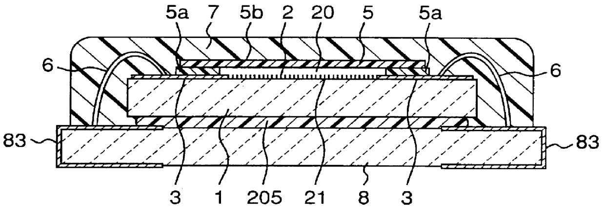
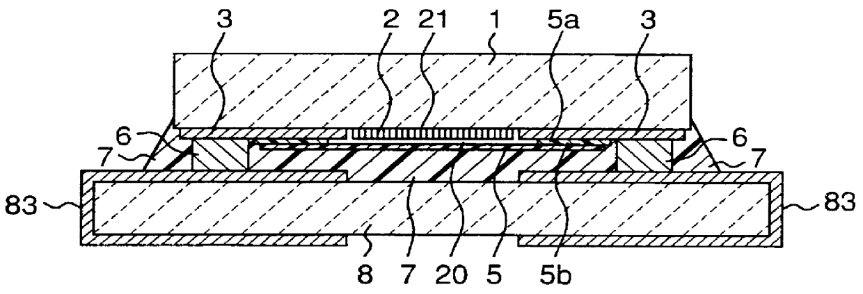
In FIGS, 1A and 1B, an acoustic surface-wave device having a surface-wave propagation surface as a functional portion 2 on a main surface 21 of a functional device chip 1 is shown as an example of an electronic part. In the acoustic surface-wave device 1, a transversal interdigital electrode is formed by using the ordinary photo-lithographic method for the functional portion. The electrode pads 3 for establishing electric conduction with an external circuit outside the functional portion is made of a metallic film mainly consisting of aluminum.

In the electronic part shown in FIG. 1A, the functional device chip 1 is equipped with a space retainer 5 for covering the functional portion 2 and for forming a hermetic space 20 therein. The opposite surface side of the chip 1 faces a circuit substrate 8 and is secured to the circuit substrate by an adhesive layer. The electrode pads 3 on the main surface 21 are connected to the wiring electrode pads 83 of the circuit substrate...

embodiment 2

(Embodiment 2)

FIGS. 5 and 6 shows examples of electronic parts wherein the functional device chip thereof is an acoustic surface-wave filter comprising five acoustic surface-wave resonators used as its functional portion 2 on a main surface 21 and connected in a ladder form. In these examples, the chip is face-down mounted on the circuit substrate.

In FIGS. 7 and 8, the support layer 5a of the space retainer 5 is formed in the same way as that described in embodiment 1. In particular, in this example, an opening 50 corresponding to each acoustic surface-wave resonator is provided in a support layer 5a. The cover 5b is a resin film having a shape for blocking all the openings 50 at a time, and then joined onto the support layer 5a by heating under pressure. However, when the lamination method is employed when processing the cover 5b, it is preferable that the support layer 5a is designed so that the area of each opening 50 is reduced in order to minimize the warp of the cover 5b.

Next,...

embodiment 3

(Embodiment 3)

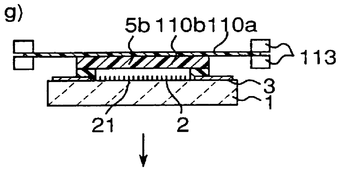
FIG. 10 shows an acoustic surface-wave device having a functional portion 2 on a main surface 21 of a functional device chip. Electrode pads 3 made of metallic film mainly consisting of aluminum are formed on the chip 1 by using the ordinary photo-lithographic method so as to establish electric conduction between an external circuit and the functional portion 2 having an interdigital electrode. Just as in the case of the embodiment 1, the support layer 5a and the film-shaped cover 5b of a space retainer 5 are formed on the chip 1 by using a dry film resist 110. Next, a metal mask having an opening corresponding to the shapes of the cover 5b and a grounding electrode pad 3a is prepared, and an isolation layer 9 made of aluminum is formed by the sputtering method.

In the isolation layer 9 made of the above-mentioned metal, the isolation layer 91 thereof for covering the support layer 5a and the side surface portion of the cover 5b is electrically connected to a grounding ...


PUM

PropertyMeasurementUnit
thicknessaaaaaaaaaa
thicknessaaaaaaaaaa
diameteraaaaaaaaaa

Abstract

The present invention relates to an electronic part used for mobile communications apparatuses and the like, and more particularly to an electronic part, such as an acoustic surface-wave device, a piezoelectric ceramic device or the like, which requires an oscillation space near the surface of the functional device chip thereof, and a method of production thereof. With this method, a space retainer for forming a sealed space at the functional portion of the chip can be hermetically sealed and have high moisture resistance, and the process of forming the space retainer can be carried out easily. The electronic part of the present invention comprises a functional device chip, a space retainer for forming a sealed space at the functional portion of the chip, a circuit substrate to which the chip is secured, electrode interconnection portions for establishing electric connection between the chip and the circuit substrate, and a sealing resin for covering and sealing at least the space retainer, wherein the space retainer comprises a support layer made of a synthetic resin film, provided with an opening enclosing the functional portion and joined onto the main surface, and a cover formed and joined onto the support layer so as to cover the functional portion and form a sealed space between the cover and the functional portion.

Description

1. Field of the InventionThe present invention relates to an electronic part used for mobile communications apparatuses and the like, and a method of production thereof, and more particularly to an electronic part, such as an acoustic surface-wave device, a crystal device or a piezoelectric ceramic device, which requires an oscillation space near the surface of the functional device chip thereof, and a method of production thereof.2. Prior ArtAs the progress of mobile communications, electronic parts, a kind of key devices constituting apparatuses, are requested to be made more compact, lower in profile and higher in performance.FIG. 20 shows the structure of a conventional electronic part having a functional portion 2 as an oscillation surface on the main surface 21 of a piezoelectric oscillation device. A functional device chip 1 is secured to a package 206 via an adhesive 205. Electric conduction between the chip 1 and the package 206 is established by electrode interconnection p...

Claims


Application Information

Patent Timeline
Patent Type & Authority Patents(United States)
IPC IPC(8): H03H3/08H03H9/10H03H9/05H03H3/00
CPCH03H3/08H03H9/0509H03H9/0585H03H9/059H03H9/1042H03H9/1071H03H9/1085H03H9/1092H01L2224/1134Y10T29/42H01L2224/13124H01L2224/13144H01L2924/09701H01L2924/16152H01L2224/131Y10T29/4913Y10T29/49146H01L2924/00013H01L2924/014H01L2924/00014H01L2224/13099H01L2224/45144
Inventor ONISHI, KEIJIIWAKI, HIDEKISEKI, SHUN-ICHITAGUCHI, YUTAKASHIRAISHI, TSUKASABESSHO, YOSHIHIROKAWASAKI, OSAMUEDA, KAZUO
Owner SKYWORKS PANASONIC FILTER SOLUTIONS JAPAN
Why Eureka
Try Eureka