Method for forming gate oxides of different thicknesses

a gate oxide and thickness technology, applied in the field of semiconductor fabrication, can solve the problems of uneven thickness, surface cleanliness, and unwanted variations in the thickness of the gate oxide in the first art approach

Inactive Publication Date: 2000-12-26
INTEGRATED DEVICE TECH INC
View PDF31 Cites 20 Cited by
  • Summary
  • Abstract
  • Description
  • Claims
  • Application Information

AI Technical Summary

Benefits of technology

A method of forming a plurality of gate oxide thicknesses, representing an embodiment of the invention, can be cost effective and advantageous for at least the following reasons. The invention provides better cleanliness, thereby yielding a better gate oxide compared to conventional processes. The invention improves device uniformity and results in better oxide quality compared to conventional processes. The invention provides gate oxides of different thicknesses without adversely affecting carrier mobility.All the disclosed embodiments of the invention described herein can be realized and practiced without undue experimentation. Although the best mode of carrying out the invention contemplated by the inventors is disclosed above, practice of the invention is not limited thereto. Accordingly, it will be appreciated by those skilled in the art that the invention may be practiced otherwise than as specifically described herein.For example, the individual components need not be formed in the disclosed shapes, or assembled in the disclosed configuration, but could be provided in virtually any shape, and assembled in virtually any configuration. Further, the individual components need not be fabricated from the disclosed materials, but could be fabricated from virtually any suitable materials. Further, although the gate oxide fabrication process described herein can be a temporally separate process, it will be manifest that the gate oxide fabrication process may be as a subprocess integrated into a larger process with which it is associated. Furthermore, all the disclosed elements and features of each disclosed embodiment can be combined with, or substituted for, the disclosed elements and features of every other disclosed embodiment except where such elements or features are mutually exclusive.It will be manifest that various additions, modifications and rearrangements of the features of the invention may be made without deviating from the spirit and scope of the underlying inventive concept. It is intended that the scope of the invention as defined by the appended claims and their equivalents cover all such additions, modifications, and rearrangements. The appended claims are not to be interpreted as including means-plus-function limitations, unless such a limitation is explicitly recited in a given claim using the phrase "means-for." Expedient embodiments of the invention are differentiated by the appended subclaims.

Problems solved by technology

The first art approach has a surface cleanliness problem due to direct contact of the gate oxide with photoresist.
The second approach also has a uniformity problem with regard to nitrogen dopant concentration.
Variations in nitrogen concentration cause unwanted variations in the resulting gate oxide thicknesses.
The second approach also has a problem with regard to stray nitrogen in the channel region, (which is near the gate oxide region) degrades carrier mobility.
Heretofore, with regard to formation of gate oxides of different thicknesses, the requirements of cleanliness, uniformity, and avoidance of carrier mobility degradation have not been fully met.

Method used


Image

  • Method for forming gate oxides of different thicknesses
  • Method for forming gate oxides of different thicknesses
  • Method for forming gate oxides of different thicknesses

Examples


first embodiment

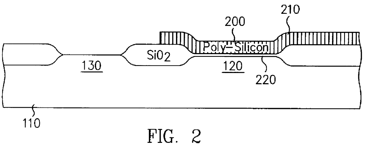
FIGS. 1-6 depict an implementation of the invention to achieve local oxidation of silicon (LOCOS) isolation. FIG. 1 depicts growing a first gate oxidation sub-layer precursor 100 on a substrate 110 having a first gate region 120 separated from a second gate region 130 by a local oxidation of silicon field 140. The substrate 110 can include silicon or any other suitable semiconductor substrate material.

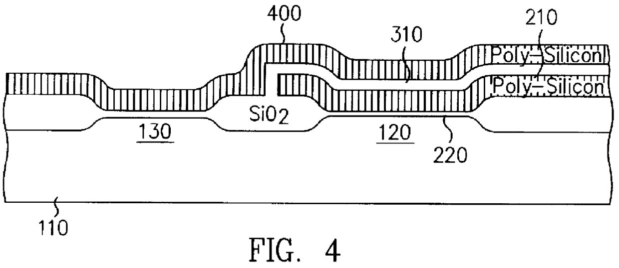
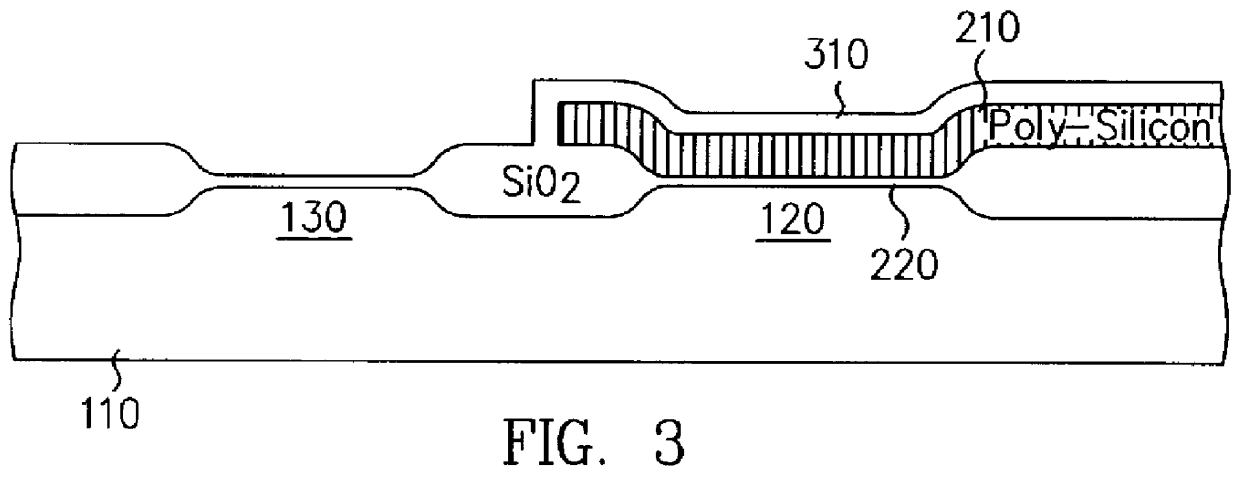
FIG. 2 shows the LOCOS device after a number of processing steps. These steps include depositing a first layer of poly-silicon on the first gate oxidation sub-layer precursor. Only the portion of this first layer of poly-silicon that remains is shown in FIG. 2. It can also be appreciated that only a portion of the first gate oxidation sub-layer precursor remains in FIG. 2. These steps also include masking a first portion of the first layer of poly-silicon 200 that overlies both i) a first portion of the first gate oxidation sub-layer precursor and ii) the first gate region 120. The mas...

second embodiment

FIGS. 7-12 depict an implementation of the invention to achieve shallow trench isolation (STI). FIG. 7 depicts growing a first gate oxidation sub-layer precursor 710 on a substrate 720 having a first gate region 740 separated from a second gate region 750 by an oxide filled trench 730. The substrate 720 can include silicon or any other suitable semiconductor substrate material. After the trench 730 is filled with oxide, the oxide can be polished back to a smooth surface, before the first gate oxidation sub-layer precursor 710 is grown.

FIG. 8 depicts the STI device after a number of additional processing steps. These processing steps include forming a first layer of poly-silicon on the first gate oxidation sub-layer precursor. The first layer of poly-silicon can be formed by deposition. These processing steps also include masking a first portion of the first layer of poly-silicon that overlies both i) a first portion of the first gate oxidation sub-layer precursor and ii) the first g...

third embodiment

FIGS. 13-16 depict an implementation of the invention to achieve local oxidation of silicon (LOCOS) isolation. FIG. 13 depicts growing a first gate oxidation sub-layer precursor 1310 on a substrate 1320 having a first gate region 1330 separated from a second gate region 1340 by a local oxidation of silicon field 1350. The substrate 1320 can include silicon or any other suitable semiconductor substrate material.

FIG. 14 depicts the LOCOS structure after a number of additional steps. These additional steps includes depositing a first layer of poly-silicon on the first gate oxidation sub-layer precursor 1310. These additional steps also include depositing a layer of silicon nitride on the first layer of poly-silicon. These additional steps also include masking a first portion of the layer of silicon nitride 1410 that overlies i) a first portion of the first layer of poly-silicon 1420, ii) a first portion of the first gate oxidation sub-layer precursor and iii) the first gate region 1330...


PUM


Abstract

Systems and methods are described for fabricating semiconductor gate oxides of different thicknesses. Two methods for forming gate oxides of different thicknesses in conjunction with local oxidation of silicon (LOCOS) are disclosed. Similarly, two methods for forming gate oxides of different thicknesses in conjunction with shallow trench isolation (STI) are disclosed. Techniques that use two poly-silicon sub-layers of substantially equal thickness and techniques that use two poly-silicon sub-layers of substantially unequal thickness are described for both LOCOS and STI. The systems and methods provide advantages because gate uniformity and quality are improved, the processes and resulting devices are cleaner, and there is less degradation of carrier mobility.

Description

1. Field of the InventionThe invention relates generally to the field of semiconductor fabrication. More particularly, the invention relates to forming gate oxides of different thicknesses.2. Discussion of the Related ArtPrior art transistor gate oxides are well known to those skilled in the art. In the past, gate oxides of different thicknesses have been formed on a single wafer.A conventional way to achieve two different gate oxide thicknesses on a single wafer is to grow an oxide with certain thickness and selectively etch certain regions. A second oxide growth is performed after the etch. Regions that were previously etched will exhibit a thinner resulting oxide. Those regions that were not etched will exhibit a thicker resulting oxide.Another conventional way to vary the gate oxide thickness on a single wafer is to implant nitrogen into the gate region before gate oxidation. The oxidation growth rate depends on the nitrogen implant dose. By selectively exposing some gate region...

Claims


Application Information

Patent Timeline
Patent Type & Authority Patents(United States)
IPC IPC(8): H01L21/70H01L21/8234
CPCH01L21/823462Y10S438/981
Inventor JIA, JAMES YINGBOCHOI, JEONG-YEOL
Owner INTEGRATED DEVICE TECH INC
Why Eureka
Try Eureka