Thin film transistors and electronic devices comprising such

Inactive Publication Date: 2001-01-30
US PHILIPS CORP
View PDF10 Cites 49 Cited by
  • Summary
  • Abstract
  • Description
  • Claims
  • Application Information

AI Technical Summary

Benefits of technology

It is an object of the present invention, therefore, to provide an electronic device having a top-gate

Problems solved by technology

The present invention is based on an appreciation by the present inventors that using a noble inert gas diluted plasma in the deposition the semiconductor layer can avoid, or at least reduce, hydrogen reduction of the underlying s

Method used


Image

  • Thin film transistors and electronic devices comprising such
  • Thin film transistors and electronic devices comprising such
  • Thin film transistors and electronic devices comprising such

Examples


Embodiment Construction

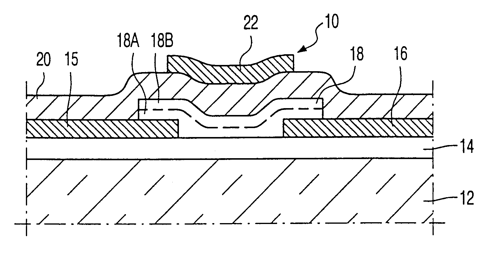
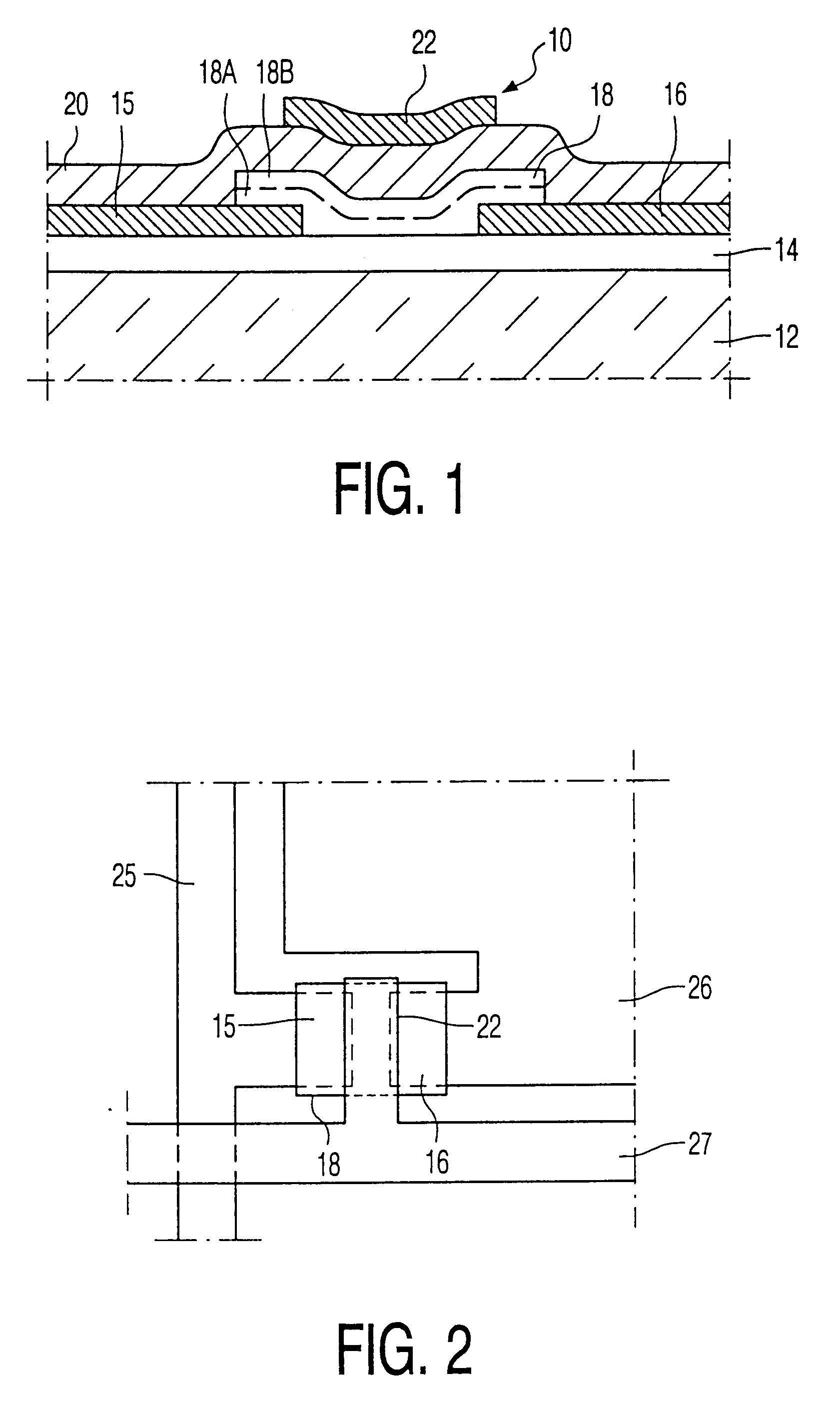
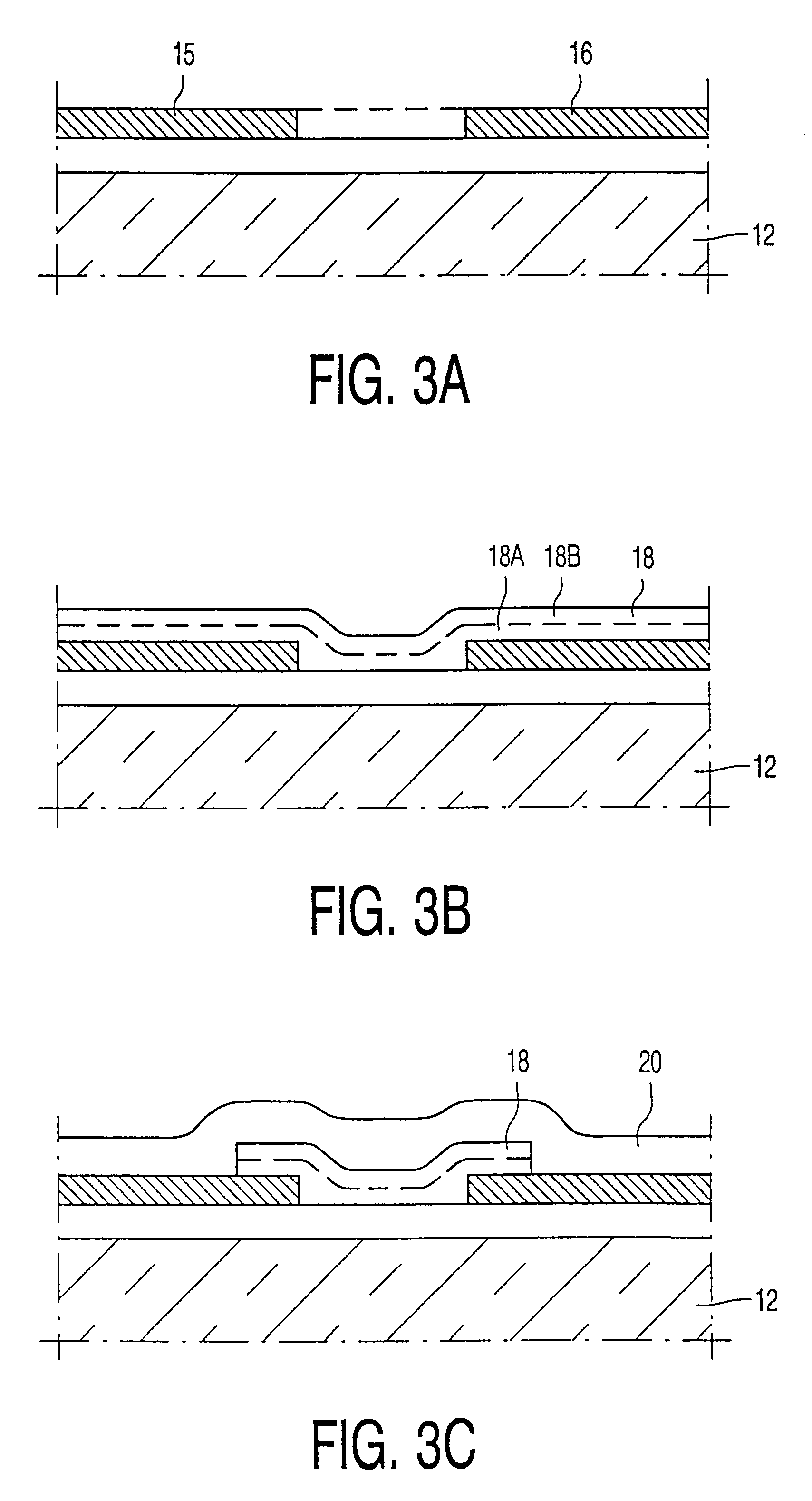
It should be understood that the Figures are merely schematic and are not drawn to scale. Certain dimensions, such as the thicknesses of layers or regions, may be shown exaggerated while other dimensions may have been reduced for the sake of clarity. The same reference numerals are used throughout the drawings to indicate the same or similar parts.

FIG. 1 illustrates a part of a large area electronic device which may be, for example, a flat panel display device of similar kind to the active matrix liquid crystal display device described in U.S. Pat. No. 5,130,829. Thus, a back plate of the display device may provide a substrate on a first major surface of which the TFT of FIG. 1, generally referenced at 10, is provided. The TFT 10 comprises an amorphous silicon TFT of the so-called top gate staggered variety. The substrate is electrically insulating at least adjacent its major surface and may comprise glass or another insulating material such as a plastics material. In this particula...


PUM


Abstract

In an electronic device, such as an active matrix display device or the like, comprising a top gate amorphous silicon thin film transistor (10) in which one or both of the source and drain electrodes (15, 16) is of transparent conductive material such as ITO, the PECVD deposited semiconductor layer (18) extending over and between the source and drain electrodes of the TFT is formed as first and second sub-layers (18A, 18B), using different source gas compositions. A noble inert gas such as helium is used as dilutant in forming the first sub-layer adjacent the source and drain electrodes to avoid reduction problems while hydrogen is used as the dilutant in forming the second sub-layer to achieve high stability and mobility characteristics in the completed transistor.

Description

BACKGROUND OF THE INVENTIONThis invention relates to electronic devices comprising a thin-film transistor and methods of manufacturing such. The device may be a flat panel display, for example, an active-matrix liquid-crystal display, or another type of large-area electronic device, for example, a large-area image sensor or touch sensor, or a thin-film data store or memory device.There is currently much interest in developing thin-film circuits with thin-film transistors (hereinafter termed "TFTs") on glass and on other inexpensive insulating substrates for large-area electronics applications. Such TFTs may form the switching elements in a cell matrix, for example in a flat panel display as described in U.S. Pat. No. 5,130,829, and / or in integrated drive circuits for such cell matrices.In the development and manufacture of large-area electronic devices, it is recognised that the performance of the TFTs can depend critically on the quality of the electrical contact between the source...

Claims


Application Information

Patent Timeline
IPC IPC(8): H01L21/02H01L21/205H01L29/66H01L21/336H01L29/786G02F1/136G02F1/1368G09F9/30
CPCH01L29/66765H01L29/78666H01L21/02422H01L21/02532H01L21/02576H01L21/0262
Inventor DEANE, STEVEN C.FRENCH, IAN D.
Owner US PHILIPS CORP
Why Eureka
Try Eureka