

Image detecting device and an X-ray imaging system
a technology of image detection and imaging system, which is applied in the direction of television system, radioation control device, instruments, etc., can solve the problems of large size of image detecting device, image quality deterioration, and inability to quickly and easily obtain digital images
- Summary
- Abstract
- Description
- Claims
- Application Information
AI Technical Summary
Problems solved by technology
Method used
Image

Examples
first embodiment
(First Embodiment)
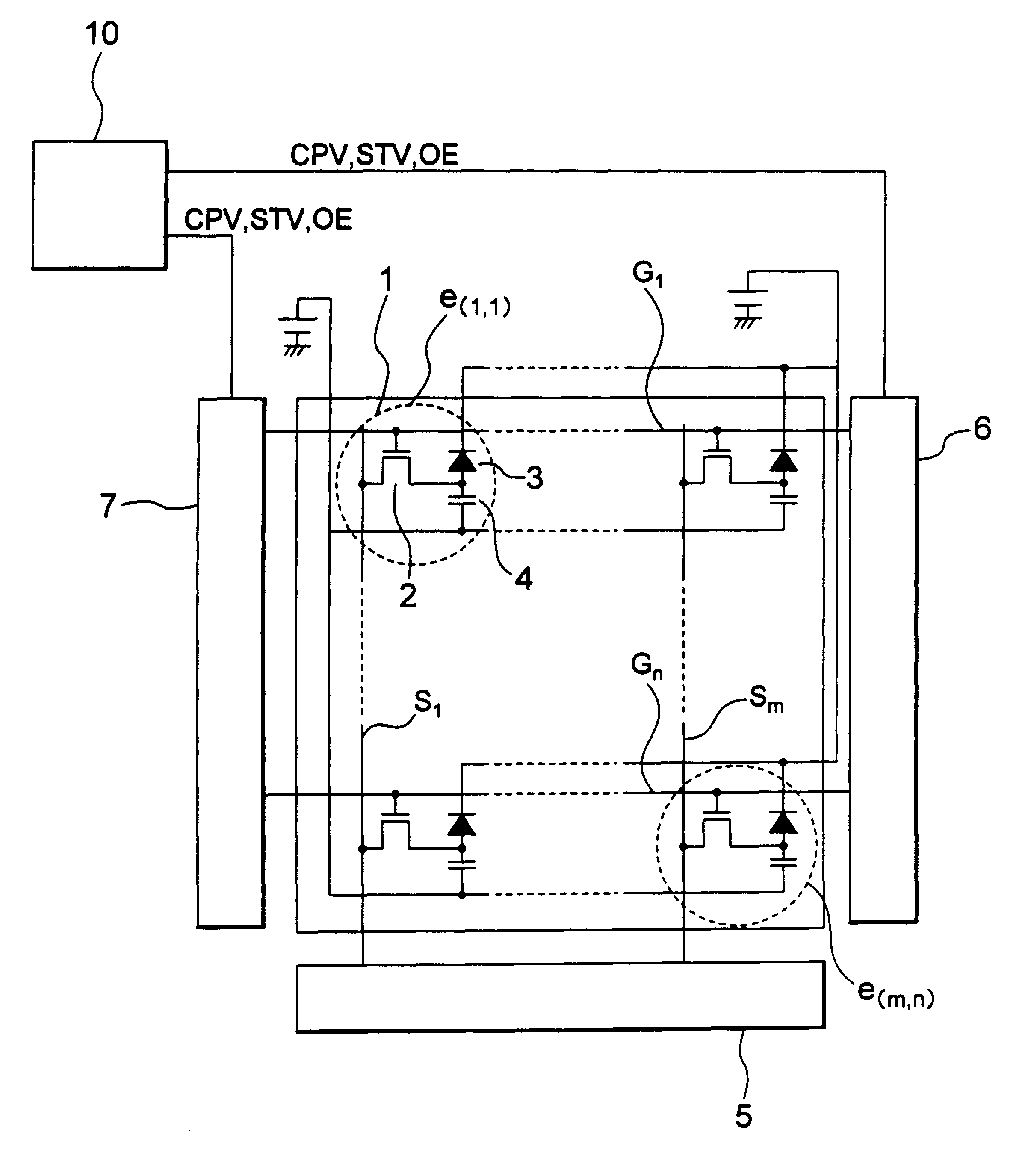
FIG. 1 is a circuit diagram showing an example of the structure of an image detecting device according to a first embodiment of the present invention.
In FIG. 1, on a TFT array 1, pixels e (m, n), signal lines Sm, and scan lines Gn are disposed. Each of the pixels e (m, n) is composed of a TFT 2, a photoelectric film 3, and a pixel capacitor 4.
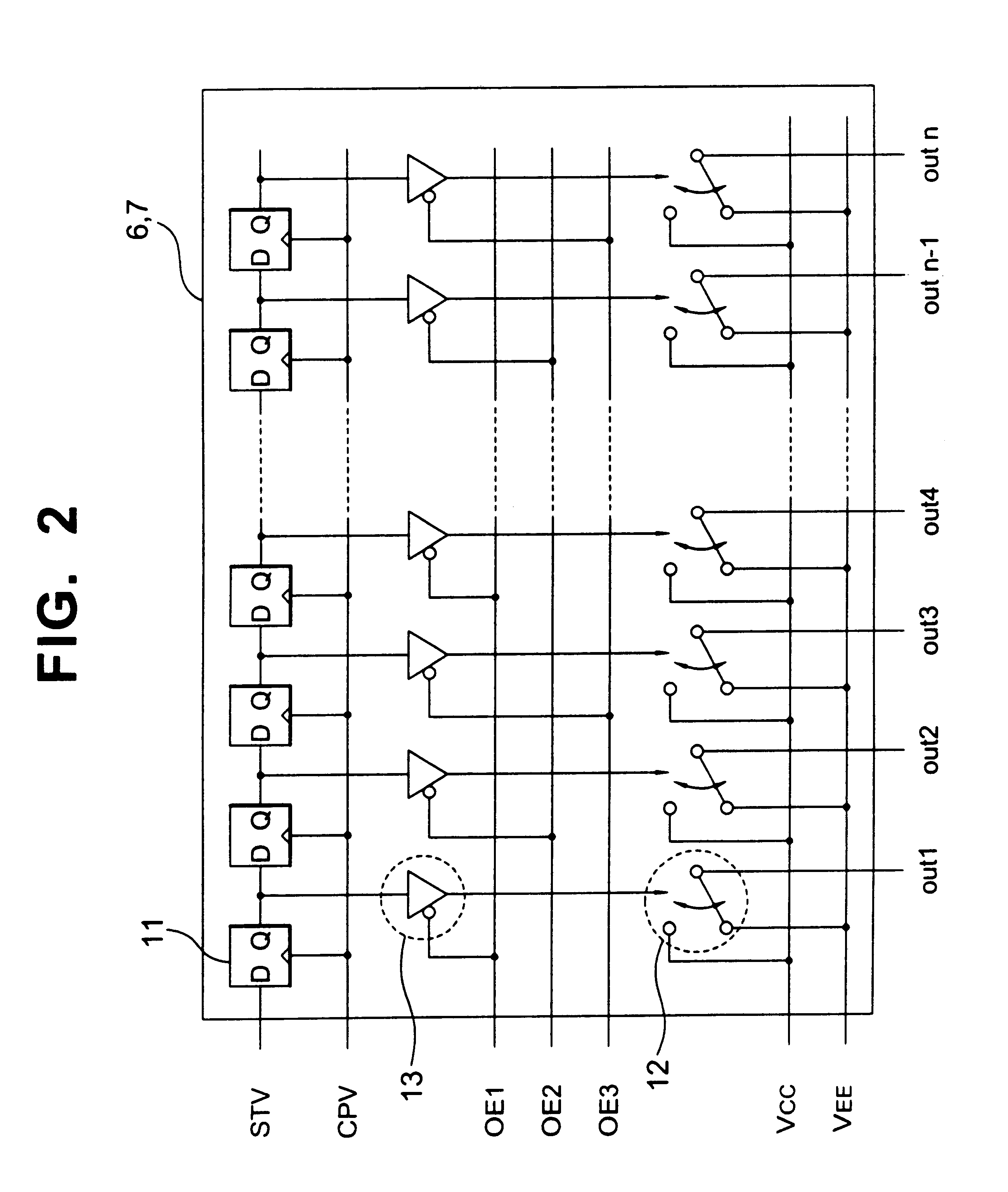
A detecting amplifier 5 and two scan line driving circuits 6 and 7 are disposed on the TFT array 1 or another substrate 9 (not shown) through an FPC cable 8 or the like (not shown). A first end side of the signal lines Sm is connected to the detecting amplifier 5. A first end side of the scan lines Gn is connected to the scan line driving circuit 6. A second end side of the scan lines Gn is connected to the scan line driving circuit 7. A control signal supplying circuit 10 supplies three types of signals that are a clock signal CPV, a start pulse STV, and an enable signal OE to the scanning line driving circuits 6 and 7.
FIG. 2...
second embodiment
(Second Embodiment)
FIG. 4 is a circuit diagram showing an example of the structure of an image detecting device according to a second embodiment of the present invention. The fundamental structure and operation of the image detecting device according to the second embodiment are the same as those according to the first embodiment. Thus, for simplicity, in FIG. 4, similar portions to those in FIG. 1 are denoted by similar reference numerals and their description will be omitted.
In FIG. 4, on a TFT array 1, pixels e (m, n), signal lines Sm, and scan lines Gn are disposed. Each of the pixels e (m, n) is composed of a TFT 2, a photoelectric film 3, and a pixel capacitor 4.
A detecting amplifier 5 and two scan line driving circuits 6 and 7 are disposed on the TFT array 1 or another substrate 9 (not shown) through an FPC cable 8 or the like (not shown). A first end side of the signal lines Sm is connected to the detecting amplifier 5.
A first end side of the scan lines Gn is connected to th...
third embodiment
(Third Embodiment)
FIG. 8 is a circuit diagram showing an example of the structure of an image detecting device according to a third embodiment of the present invention. The fundamental structure and operation of the image detecting device according to the third embodiment are the same as those according to the first embodiment. For simplicity, in FIG. 8, similar portions to those in FIG. 1 are denoted by similar reference numerals and their description will be omitted.
In the third embodiment, the scan line driving circuit 6 of the second embodiment is connected to the first end side of the scan lines. As with the second embodiment, in the third embodiment, the period for selecting one scan line becomes long. Thus, since the influence against signal delays and waveform distortion can be alleviated, an image detecting device with a high frame rate can be accomplished.
PUM
 Abstract
Description
Claims
Application Information