Method of fabrication of an infrared radiation detector and infrared detector device

a technology of infrared radiation and detector device, which is applied in the direction of sustainable manufacturing/processing, instruments, optical radiation measurement, etc., can solve the problem of incompatibility of bulk micro-machining with standard ic fabrication techniques

Inactive Publication Date: 2001-02-27
INTERUNIVERSITAIR MICRO ELECTRONICS CENT (IMEC VZW)
View PDF10 Cites 171 Cited by
  • Summary
  • Abstract
  • Description
  • Claims
  • Application Information

AI Technical Summary

Benefits of technology

As a second aspect, the present invention is related to a method of controlling stress in a polycrystalline SiGe layer d...

Problems solved by technology

Double-sided processing and special handling requirements though make...

Method used


Image

  • Method of fabrication of an infrared radiation detector and infrared detector device
  • Method of fabrication of an infrared radiation detector and infrared detector device
  • Method of fabrication of an infrared radiation detector and infrared detector device

Examples


Embodiment Construction

In an aspect of the present invention, a method of fabricating an infrared bolometer is described, which has an improved thermal insulation behaviour. Furthermore, a bolometer fabricated according to the method of the invention is described.

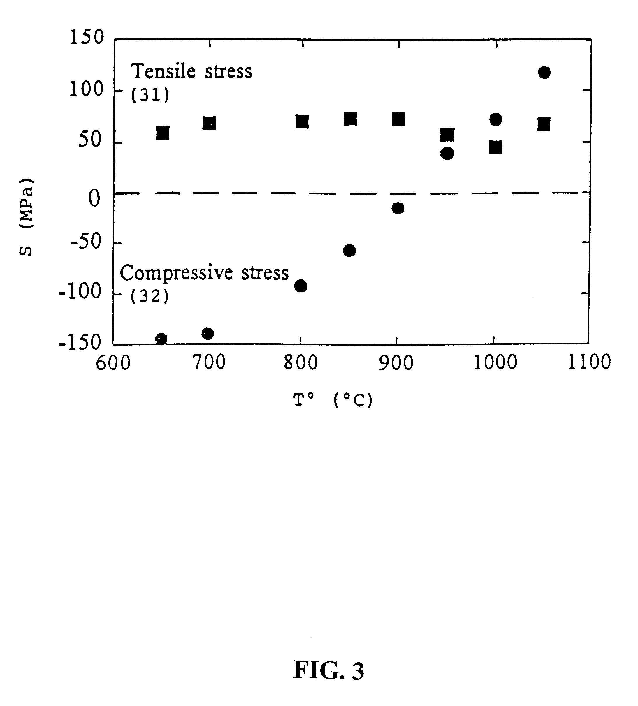
In order to evaluate a material for the realisation of a bolometer, it is necessary to understand how its properties influence the responsivity and the noise of the bolometer itself.

According to the invention, use is made of an alloy comprising polycrystalline Silicon Germanium (poly-SiGe).

This material has lower thermal conductance than polycrystalline silicon, and is compatible with the standard IC technology. It also has electrical and mechanical properties which are superior to those of polycrystalline silicon.

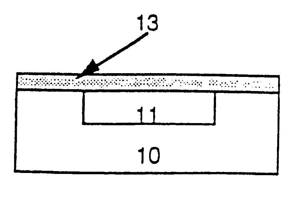
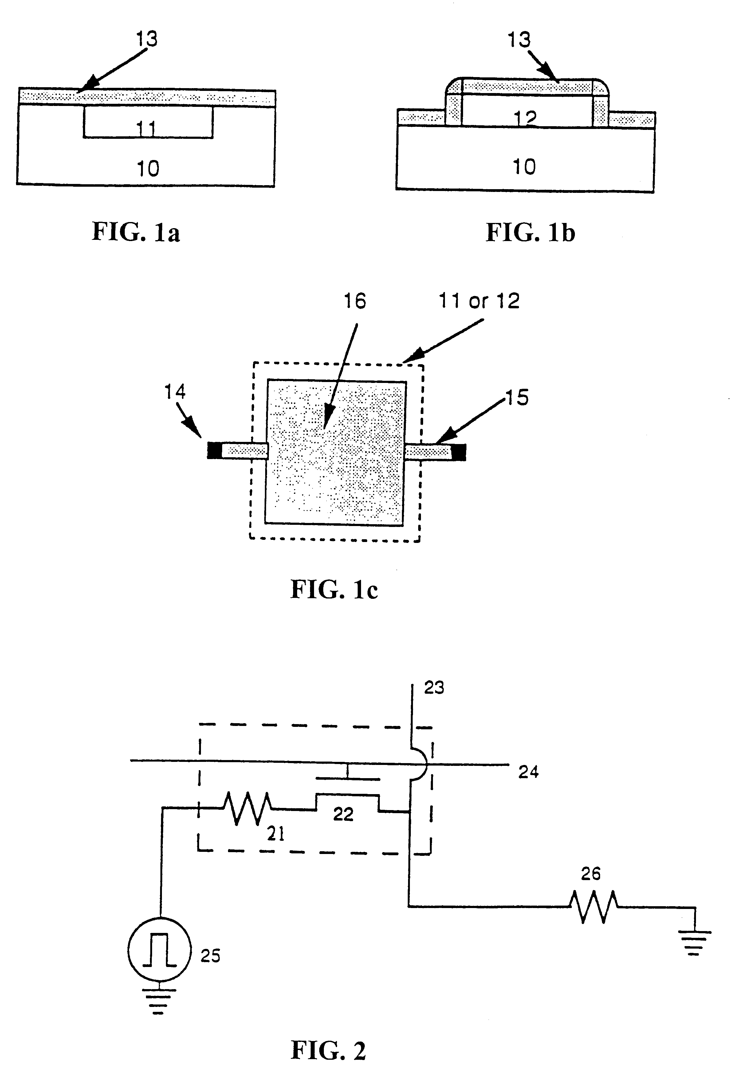
Several possible structures of bolometers are shown in the FIGS. 1a, 1b, and 1c.

FIG. 1a represents a bolometer wherein porous silicon regions 11 have been formed on a substrate 10, while FIG. 1b represents the deposition and the pattern...


PUM

PropertyMeasurementUnit
Pressureaaaaaaaaaa
Areaaaaaaaaaaa
Sensitivityaaaaaaaaaa

Abstract

A method of fabricating an infrared detector, a method of controlling the stress in a polycrystalline SiGE layer and an infrared detector device is disclosed. The method of fabricating includes the steps of forming a sacrificial layer on a substrate; patterning said sacrificial layer; establishing a layer consisting essentially of polycrystalline SiGe on said sacrificial layer; depositing an infrared absorber on said polycrystalline SiGe layer; and thereafter removing the sacrificial layer. The method of controlling the stress in a polycrystalline SiGe layer deposited on a substrate is based on varying the deposition pressure. The infrared detector device comprises an active area and an infrared absorber, wherein the active area comprises a polycrystalline SiGe layer, and is suspended above a substrate.

Description

REFERENCE TO RELATED APPLICATIONSThis application claims priority to European patent application number 97870044.1 filed on Mar. 28, 1997.OBJECT OF THE INVENTIONThe present invention is related to a method of fabrication for an infrared radiation detector, and more particularly an infrared sensitive bolometer, using micro-machining techniques.The present invention is also related to the infrared detector itself.Finally, the present invention is related to a specific use of surface micro-machining techniques.A large number of infrared detection methods exist, each being based on a different working principal. Infrared detectors are being used in a large number of applications.The present invention focuses on the group of detectors where the energy of the absorbed infrared radiation raises the temperature of the detecting element thereby changing its electrical conductivity. These detectors, known as bolometers, are fabricated from different materials like metals, permalloy, vanadium ...

Claims


Application Information

Patent Timeline
IPC IPC(8): B81B3/00G01J5/20H01L31/09H01L31/08H01L31/18G01J1/02B81C1/00H01L31/0248
CPCB81C1/00666G01J5/20H01L31/09H01L31/1804B81C2201/017Y02E10/547Y02P70/50
Inventor FIORINI, PAOLOSEDKY, SHERIFCAYMAX, MATTYBAERT, CHRISTIAAN
Owner INTERUNIVERSITAIR MICRO ELECTRONICS CENT (IMEC VZW)
Why Eureka
Try Eureka