Constrained register sharing technique for low power VLSI design
a register sharing and low power technology, applied in the direction of cad circuit design, program control, instruments, etc., can solve the problems of large fraction of unnecessary power dissipation, components may be idle in some clock cycles, and large amount of such transitions incurred during the operation of commonly used circuits, so as to avoid unnecessary switching operations
- Summary
- Abstract
- Description
- Claims
- Application Information
AI Technical Summary
Benefits of technology
Problems solved by technology
Method used
Image
Examples
example 1
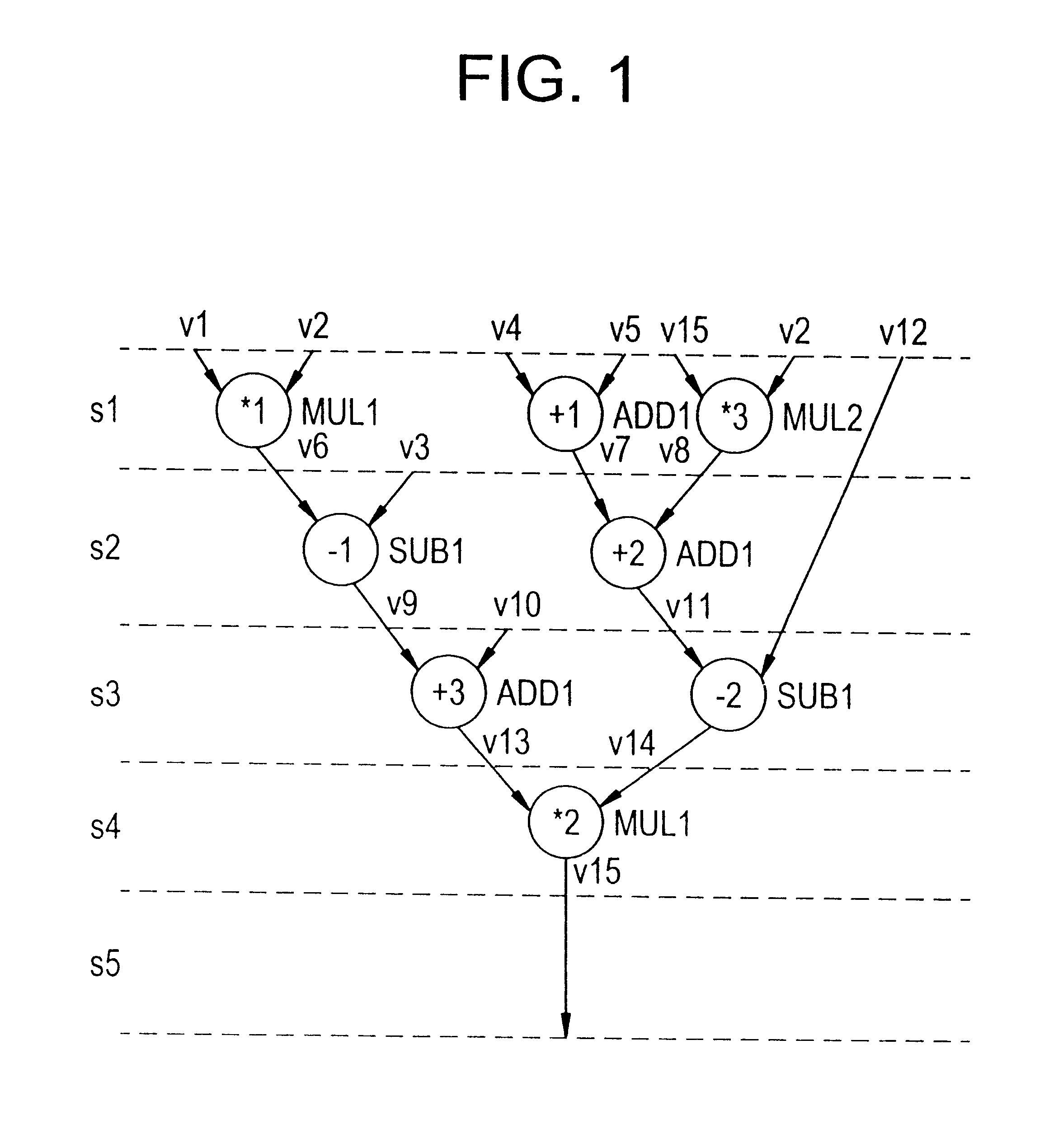
Consider the scheduled CDFG shown in FIG. 1. Each operation in the CDFG is annotated with its name (placed inside the circle representing the operation) and the name of the functional unit instance it is mapped to (placed outside the circle representing the operation). Each variable in the CDFG is annotated with its name. Clock cycle boundaries are denoted by dotted lines. The schedule has five control steps, s1, . . . , s5. Control step s5 is used to hold the output values in the registers and communicate them to the environment that the design interacts with, and to load the input values into their respective registers for the next iteration.
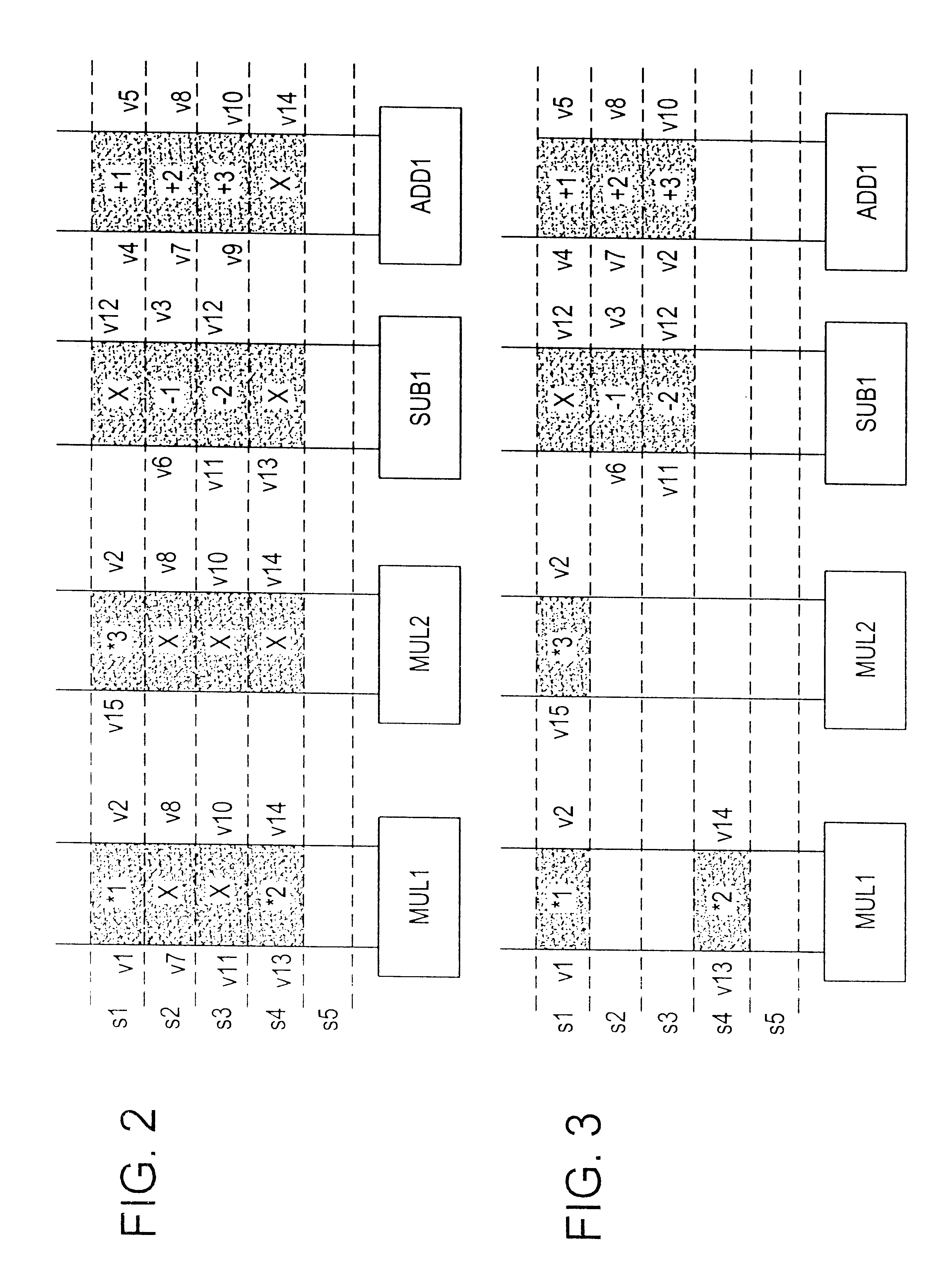
To assess the impact of variable assignment on power consumption, consider two candidate assignments, Assignment 1 and Assignment 2, shown in Table 1. The architectures obtained using these assignments were subject to logic synthesis optimizations, and placed and routed using a 1.2 micron standard coil library. The transistor-level netlists ex...
example 2
The previous example illustrated that constrained register sharing can significantly reduce the number of spurious operations m a circuit. This example illustrates another technique, called dynamic register rebinding which, in combination with variable assignment, can further eliminate spurious operations.
Consider functional unit SUB1 in Design 2. An inspection of FIG. 3 reveals that it executes a spurious operation in control step s1 of every iteration. This is because the multiplexer at its input selects register R5, to which variable v12 is assigned, from control step s3 of each iteration to control step s1 of the next iteration. Since v12 acquires a new value in control step s1 of each iteration, SUB1 computes v11-v12 in control step s1, which is spurious, since the value of v11 corresponds to the previous iteration while the value of v12 corresponds to the current iteration. This problem would persist even if v3 were selected at the input of SO B1, instead of v12. This is becau...
example 3
Consider the scheduled CDFG shown in FIG. 5. Table 2 shows two candidate variable assignments, Assignment 1 and Assignment 2, both of which require the same number of registers. Upon synthesis, the architectures corresponding to the two designs were simulated with typical input traces to determine the power consumption.
The architecture derived using the variable assignment shown in Assignment 1 consumed 42.86 mW, while the architecture derived using Assignment 2 consumed 34.05 mW. It can be seen that, for the design obtained from Assignment 1, functional unit MUL1 executes spurious operations in cycles s2 and s3, and functional unit ADD1 executes a spurious operation in cycle s4. For the design obtained from Assignment 2, the chosen variable assignment is such that no spurious operations are executed.
The above examples serve to illustrate that judicious variable assignment is a key factor in the elimination of spurious operations. The present invention aims to eliminate spurious ope...
PUM
 Abstract
Description
Claims
Application Information


