Process for producing infrared emitting device and infrared emitting device produced by the process

Inactive Publication Date: 2001-03-20
ANRITSU CORP
View PDF6 Cites 17 Cited by
  • Summary
  • Abstract
  • Description
  • Claims
  • Application Information

AI Technical Summary

Benefits of technology

The present invention has been made to solve the problems in the prior art, and has as its object to provide an infrared-emitting element manufacturing method capable of efficiently manufacturing, with high mass productivity at low cost, a high-performance infr

Problems solved by technology

In an infrared-emitting element using a ceramic bulk material as a heat-generating element, however, infrared rays cannot be modulated at a high frequency because the thermal conductivity of a high-temperature portion is small, and the heat capacity of the bulk material is large.
In the infrared-emitting element using the silicon micromachining, since the p.sup.+ -type layer is formed by thermally diffusing boron, the bridge portion of the bridge-building structure is too thick, resulting in poor thermal response characteristics for the driving power.
However, when the bridge portion obtained by thermally diffusing boron is decreased in thickness to about the reciprocal of the absorption coefficient at a necessary infrared wavelength, the emissivity of infrared rays rapidly decreases to weaken the infrared emission intensity.
In the conventional infrared-emitting element using the silicon micromachining obt

Method used


Image

  • Process for producing infrared emitting device and infrared emitting device produced by the process
  • Process for producing infrared emitting device and infrared emitting device produced by the process
  • Process for producing infrared emitting device and infrared emitting device produced by the process

Examples


Embodiment Construction

The present invention will be generally described.

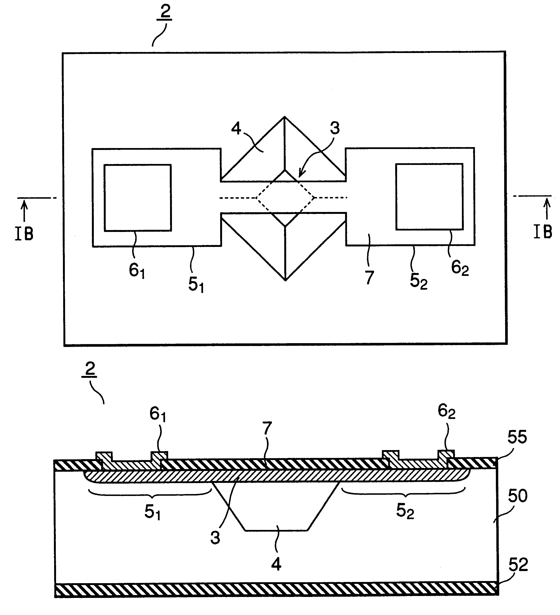
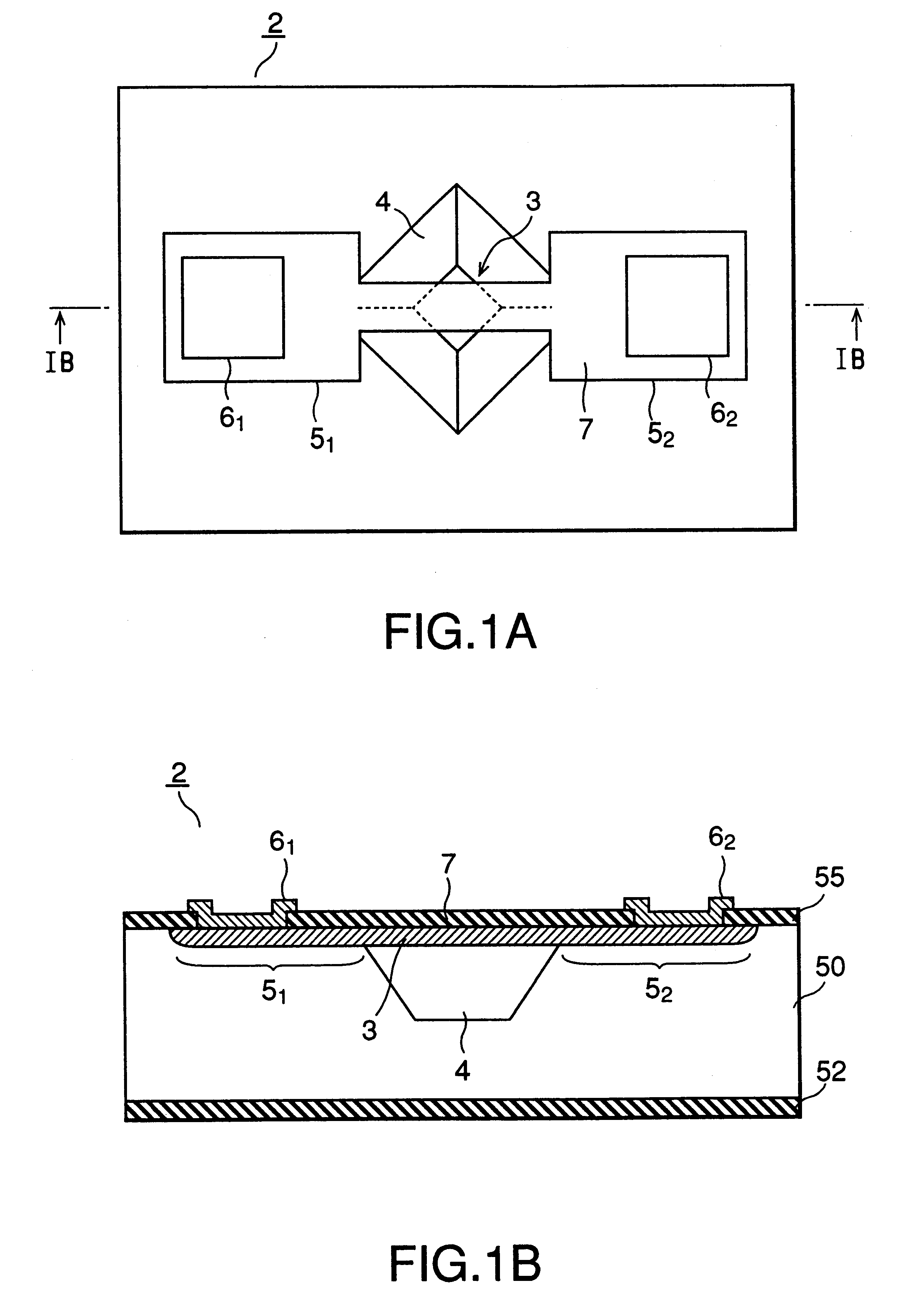
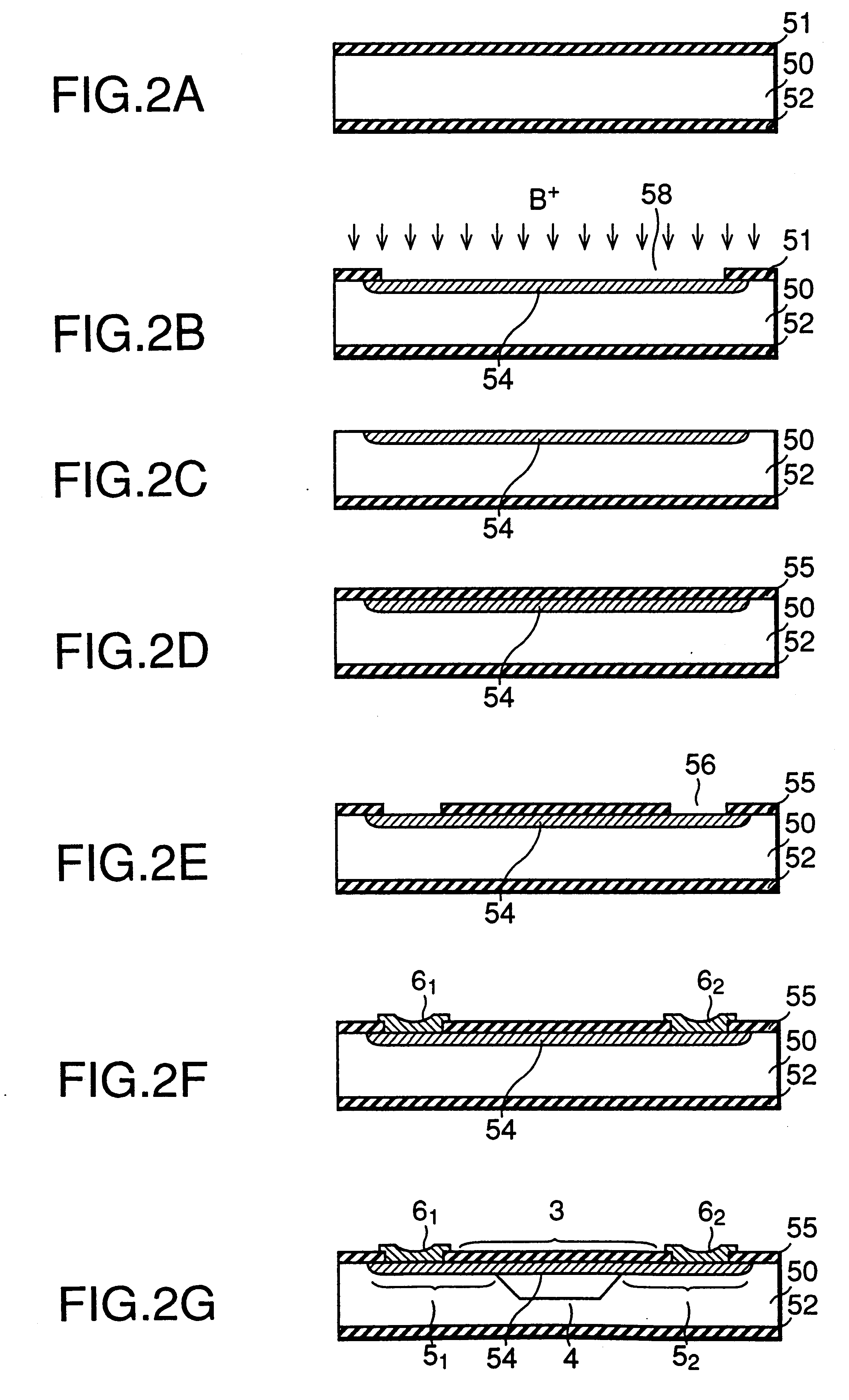
(1) To achieve the above object, the present invention is characterized by a method of manufacturing an infrared-emitting element which has an element substrate and a bridge (heat-generating) portion formed on the element substrate and shaped into a bridge-building structure by a separation space, and can emit infrared rays upon energization by a power supply, and an infrared-emitting element manufactured by the above method in which the bridge portion is formed to have a thickness of, e.g., 5 .mu.m or less, and which is manufactured as an infrared-emitting element having a heavily doped region prepared by doping an impurity by ion implantation and subsequent annealing at a dose of 3.0.times.10.sup.14 ions / cm.sup.2 or more.

(2) The present invention is characterized by a method of manufacturing an infrared-emitting element which has an element substrate and a bridge portion formed on the element substrate and shaped into a bridge-buil...


PUM


Abstract

In order, to manufacture a high-performance infrared-emitting element having high-speed thermal response characteristics and a high infrared emissivity, a bridge (heat-generating) portion having a separation space is formed on a silicon element substrate. The bridge portion is formed to have a thickness of 5 mum or less by doping boron as an impurity by ion implantation with a concentration distribution peak value of 1.5x10¹⁹ atoms/cm3 or more, and performing annealing under predetermined conditions for activating the impurity layer. In the infrared-emitting element manufactured in this manner, even if the bridge portion is made thin to improve the thermal response characteristics, the infrared emissivity does not decrease because of a high impurity concentration, and a large temperature modulation width can be obtained. In doping boron as the impurity by ion implantation, the dose is preferably set to 3.0x10¹⁴ ions/cm2 or more. To activate the impurity layer upon doping boron, the annealing is performed in the nitrogen gas atmosphere at a temperature of 1,100° C. to 1,200° C. for 5 min to 40 min and further in the wet oxygen atmosphere for about 25 min to 40 min. As a result, the doping concentration of boron by ion implantation and the activation of the impurity layer can be stably increased and enhanced.

Description

The present invention relates to an infrared-emitting element manufacturing method and an infrared-emitting element manufactured thereby and, more particularly, to a method of manufacturing an infrared-emitting element for emitting infrared rays by causing a bridge (heat-generating) portion made up of a silicon micromachining to generate heat, and an infrared-emitting element manufactured thereby.As an infrared-emitting element used for a gas analysis sensor or the like, an infrared-emitting element for emitting infrared rays from a filament by energizing the filament to make it generate heat has conventionally been used.Reference numeral 101 in FIG. 22 denotes a conventional gas analysis system using an infrared-emitting element 102 with a filament.More specifically, in this gas analysis system, infrared rays 141 emitted by the filament of the infrared-emitting element 102 are intermittently shielded by a chopper 142, and become modulated infrared rays 144, which enter a gas 143 vi...

Claims


Application Information

Patent Timeline
IPC IPC(8): G01J3/10G01J3/00H05B3/00H05B3/10
CPCG01J3/108H05B3/0047H05B3/10H05B2203/032
Inventor KODATO, SETSUOOHYA, SEISHIROKARASAWA, SHIROYUASA, HIROYASUAKIMOTO, KENJI
Owner ANRITSU CORP
Why Eureka
Try Eureka