Dual damascene metallization

a technology of damascene and metallization method, which is applied in the direction of resistive material coating, solid-state device coating, chemical vapor deposition coating, etc., can solve the problems of higher resistivity of aluminum, problems with electromigration, and opening in the circuit, so as to achieve the effect of improving the resistance and improving the resistan

Inactive Publication Date: 2001-03-27
APPLIED MATERIALS INC
View PDF34 Cites 122 Cited by
  • Summary
  • Abstract
  • Description
  • Claims
  • Application Information

AI Technical Summary

Problems solved by technology

However, aluminum has higher resistivity and problems with electromigration.
The metal gets transported from one end to the other after hours of operation and eventually separates completely, causing an opening in the circuit.
This problem is sometimes overcome by Cu doping and texture improvement.
However, electromigration is a problem that gets worse as the current density increases.
However, the primary problems with integrating copper metal into multilevel metallization systems are (1) the difficulty of patterning the metal using etching techniques, and (2) the difficulty in filling small vias using PVD given the lack of mature CVD processes.
For devices of submicron minimum feature size, wet etch techniques for copper patterning have not been acceptable due to liquid surface tension, isotropic etch profile, and difficulty in over-etch control and a reliable dry etch process is not available.
However, a reliable and mature process for selective CVD copper is not available.
However, there are two primary difficulties associated with blanket CVD processes.
First, blanket CVD films grow from all sides in an aperture which typically results in a void in the filled aperture because the deposited layer grows upwardly and outwardly at the upper comers of the aperture and bridges at the upper surface of th

Method used


Image

  • Dual damascene metallization
  • Dual damascene metallization
  • Dual damascene metallization

Examples


Embodiment Construction

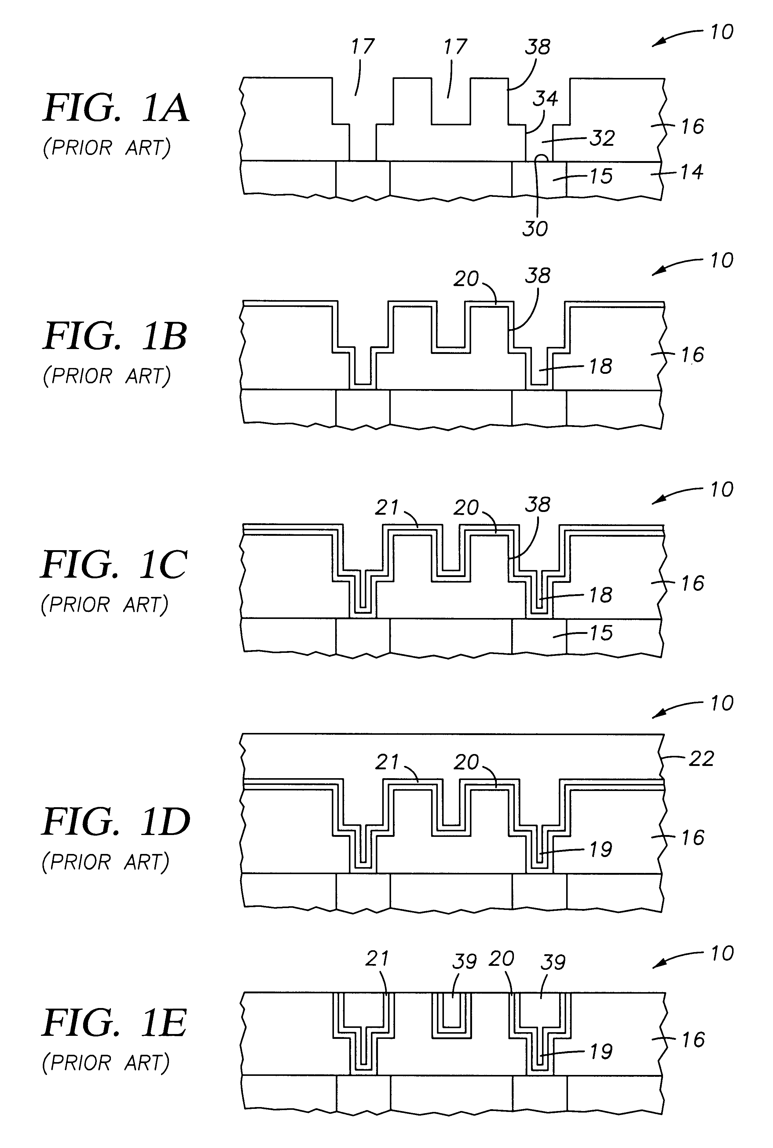
The present invention generally provides an in-situ metallization process providing an interconnect in a highly integrated structure which has a reduced interconnect resistance and improved electromigration performance. More particularly, the present invention provides a dual damascene interconnect that incorporates a barrier layer on exposed surfaces of a via and wire definition and two or more deposition techniques to fill the via and wire definition. Preferred deposition techniques can be combined in an integrated processing system, although non-integrated techniques will provide suitable metal interconnects and metal via plugs.

For clarity, the present invention will be described below with reference to copper deposition techniques. However, other metal processes, such as PVD aluminum or Al / Cu, may be used to accomplish the advantages of the present invention.

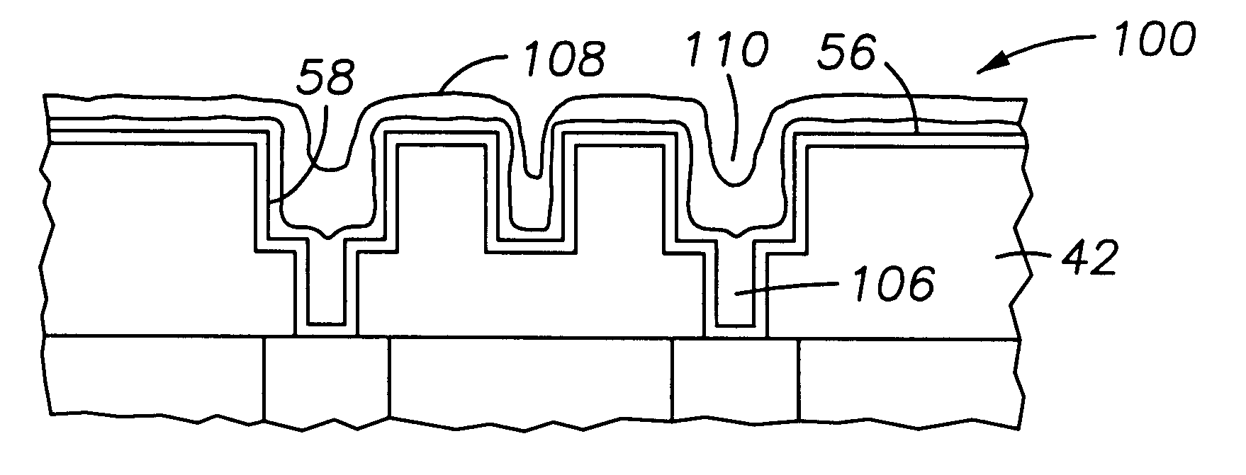
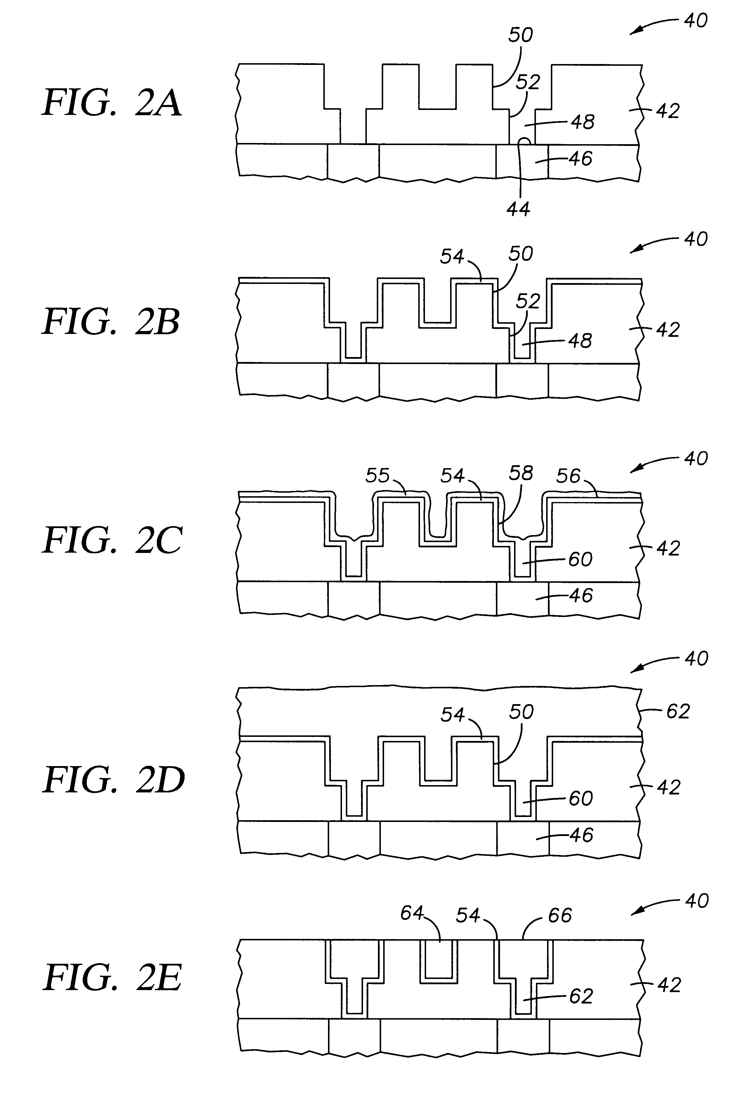
Referring to FIG. 2A, to form an IC structure 40 in accordance with the present invention, a dielectric layer 42 is formed...


PUM

PropertyMeasurementUnit
Electrical conductoraaaaaaaaaa

Abstract

The present invention generally provides a metallization process for forming a highly integrated interconnect. More particularly, the present invention provides a dual damascene interconnect module that incorporates a barrier layer deposited on all exposed surface of a dielectric layer which contains a dual damascene via and wire definition. A conductive metal is deposited on the barrier layer using two or more deposition methods to fill the via and wire definition prior to planarization. The invention provides the advantages of having copper wires with lower resistivity (greater conductivity) and greater electromigration resistance than aluminum, a barrier layer between the copper wire and the surrounding dielectric material, void-free, sub-half micron selective CVD Al via plugs, and a reduced number of process steps to achieve such integration.

Description

1. Field of the InventionThe present invention relates to a metallization method for manufacturing semiconductor devices. More particularly, the present invention relates to metallization of dual damascene via and wire definitions in a dielectric layer to form metal interconnects and metal via plugs.2. Background of the Related ArtSub-half micron multilevel metallization is one of the key technologies for the next generation of very large scale integration (VLSI). The multilevel interconnects that lie at the heart of this technology require planarization of interconnect features formed in high aspect ratio apertures, including contacts, vias, lines or other features. Reliable formation of these interconnect features is very important to the success of VLSI and to the continued effort to increase circuit density and quality on individual substrates and die.As circuit densities increase, the widths of vias, contacts and other features, as well as the dielectric materials between them,...

Claims


Application Information

Patent Timeline
IPC IPC(8): H01L21/768H01L21/70H01L21/3205H01L23/52
CPCH01L21/76831H01L21/76843H01L21/76862H01L21/76876H01L21/76877H01L21/76807
Inventor CHEN, LIANG-YUHTAO, RONGGUO, TEDMOSELY, RODERICK CRAIG
Owner APPLIED MATERIALS INC
Why Eureka
Try Eureka